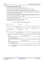
CHAPTER 14 SERIAL ARRAY UNIT
Page 351 of 920
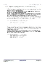
14.3.15 Registers controlling port functions of serial input/output pins
Using the serial array unit requires setting of the registers that control the port functions multiplexed on the target
channel (port mode register (PMxx), port register (Pxx), port input mode register (PIMxx), port output mode
register (POMxx), port mode control register (PMCxx)).
For details, see
5.3.1 Port mode registers (PMxx)
,
5.3.5 Port output mode registers (POMxx)
.
Specifically, using a port pin with a multiplexed serial data or serial clock output function (e.g. P02/SO10/TxD1)
for serial data or serial clock output, requires setting the corresponding bits in the port mode control register
(PMCxx) and port mode register (PMxx) to 0, and the corresponding bit in the port register (Pxx) to 1.
When using the port pin in N-ch open-drain output (V
DD
tolerance) mode, set the corresponding bit in the port
output mode register (POMxx) to 1. When connecting an external device operating on a different potential (1.8 V,
2.5 V, or 3 V), see
5.4.4 Handling different potential (1.8 V, 2.5 V, 3 V) by using I/O buffers
Example
When P02/SO10/TxD1 is to be used for serial data output
Set the PMC02 bit of port mode control register 0 to 0.
Set the PM02 bit of port mode register 0 to 0.
Set the P02 bit of port register 0 to 1.
Specifically, using a port pin with a multiplexed serial data or serial clock input function (e.g. P03/SI10/RxD1) for
serial data or serial clock input, requires setting the corresponding bit in the port mode register (PMxx) to 1, and
the corresponding bit in the port mode control register (PMCxx) to 0. In this case, the corresponding bit in the
port register (Pxx) can be set to 0 or 1.
When the TTL input buffer is selected, set the corresponding bit in the port input mode register (PIMxx) to 1.
When connecting an external device operating on a different potential (1.8 V, 2.5 V or 3 V), see
different potential (1.8 V, 2.5 V, 3 V) by using I/O buffers
Example
When P03/SI10/RxD1 is to be used for serial data input
Set the PMC03 bit of port mode control register 0 to 0.
Set the PM03 bit of port mode register 0 to 1.
Set the P03 bit of port register 0 to 0 or 1.
Summary of Contents for RL78/G1H
Page 941: ...R01UH0575EJ0120 RL78 G1H...


