


ML610471/472/473/Q471/Q472/Q473 User's Manual
Chapter 11 UART
11-9
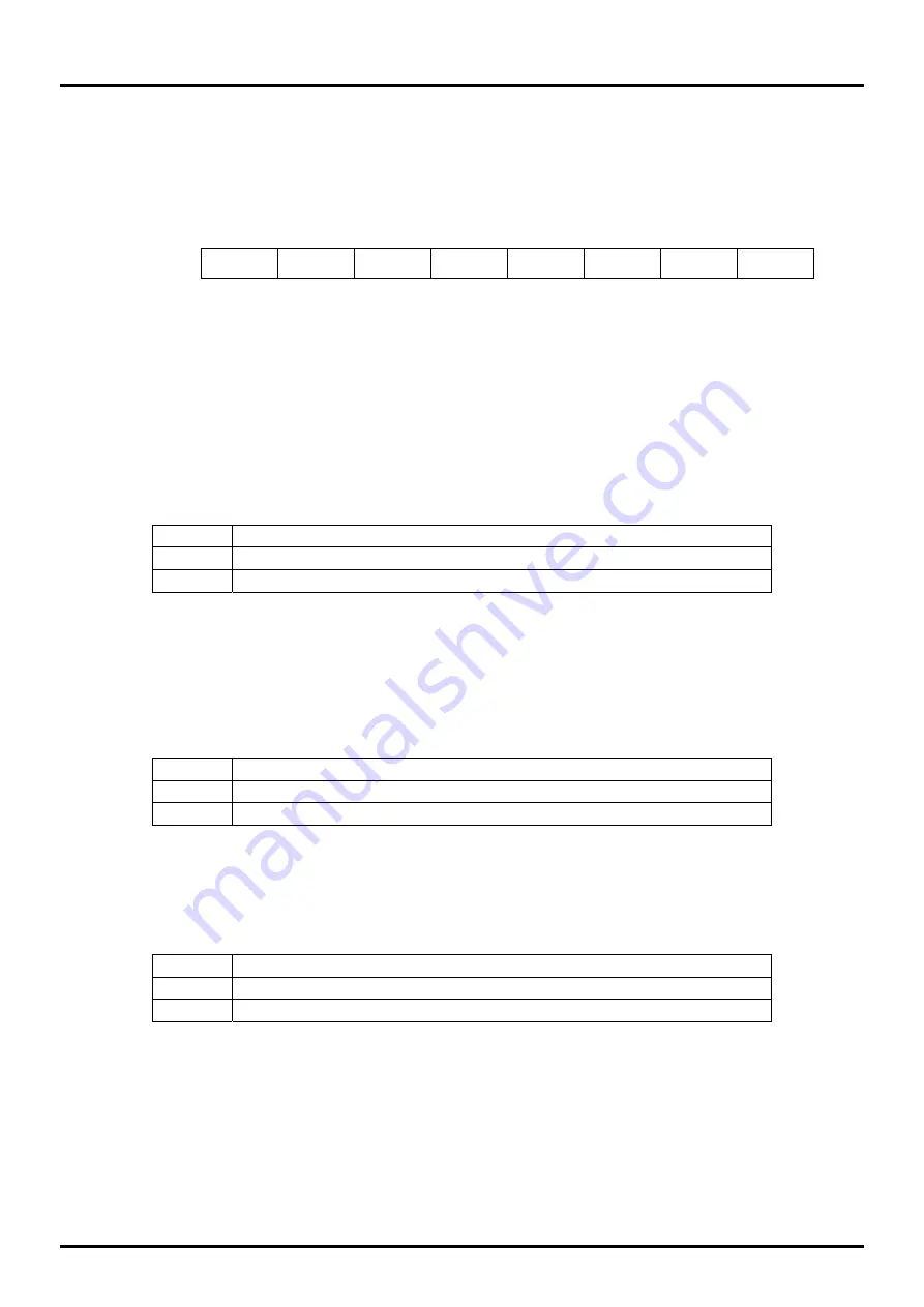
11.2.7 UART0 Status Register (UA0STAT)
Address: 0F296H
Access: R/W
Access size: 8-bit
Initial value: 00H
7 6 5 4 3 2 1 0
UA0STAT
−
−
−
−
U0FUL
U0PER
U0OER
U0FER
R/W R/W R/W R/W R/W R/W R/W R/W R/W
Initial
value
0 0 0 0 0 0 0 0
UA0STAT is a special function register (SFR) to indicate the state of transmit or receive operation of the UART.
When any data is written to UA0STAT, all the flags are initialized to “0”.
[Description of Bits]
•
U0FER
(bit 0)
The U0FER bit is used to indicate occurrence of a framing error of the UART.
When an error occurs in the start or stop bit, the U0FER bit is set to “1”. This bit is updated each time reception
is completed.
The U0FER bit is fixed to “0” in transmit mode.
U0FER
Description
0
No framing error (initial value)
1
With framing error
•
U0OER
(bit 1)
The U0OER bit is used to indicate occurrence of an overrun error of the UART.
If the received data in the transmit/receive buffer (UA0BUF) is received again before it is read, this bit is set to
“1”. Even if reception is stopped by the U0EN bit and then reception is restarted, this bit is set to “1” unless the
previously received data is not read. Therefore, make sure that data is always read from the transmit/receive
buffer even if the data is not required.
The U0OER bit is fixed to “0” in transmit mode.
U0OER
Description
0
No overrun error (initial value)
1 Overrun
error
•
U0PER
(bit 2)
The U0PER bit is used to indicate occurrence of a parity error of the UART.
When the parity of the received data and the parity bit attached to the data do not coincide, this bit is set to “1”.
U0PER is updated whenever data is received.
The U0PER bit is fixed to “0” in transmit mode.
U0PER
Description
0
No parity error (initial value)
1 Parity
error
Summary of Contents for ML610472
Page 12: ...Chapter 1 Overview...
Page 38: ...Chapter 2 CPU and Memory Space...
Page 44: ...Chapter 3 Reset Function...
Page 48: ...Chapter 4 MCU Control Function...
Page 62: ...Chapter 5 Interrupts...
Page 82: ...Chapter 6 Clock Generation Circuit...
Page 94: ...Chapter 7 Time Base Counter...
Page 105: ...Chapter 8 Capture...
Page 114: ...Chapter 9 Timer...
Page 133: ...Chapter 10 Watchdog Timer...
Page 141: ...Chapter 11 UART...
Page 164: ...Chapter 12 Port 0...
Page 173: ...Chapter 13 Port 2...
Page 180: ...Chapter 14 Port 3...
Page 188: ...Chapter 15 Port 4...
Page 199: ...Chapter 16 Port 6...
Page 205: ...Chapter 17 RC Oscillation Type A D Converter...
Page 225: ...Chapter 18 LCD Drivers...
Page 243: ...Chapter 19 Power Supply Circuit...
Page 245: ...Chapter 20 uEASE Flash Writer System...
Page 249: ...Chapter 21 Software Development...
Page 258: ...Appendixes...
Page 280: ...Revision History...


