background image


CPLD and FPGA

ATCA-8310 Installation and Use (6806800M72D

)

408

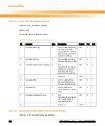
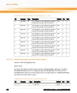
This register monitors the Reset status of 10 DSPs.

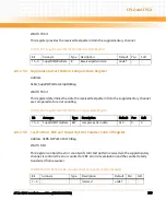
8.4.2.7.3 DSP Watchdog Interrupt Status Register

Address: 0xA4, DspWdgStaReg

Width: 16 bit

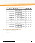
This register monitors the Watchdog Interrupt status of 10 DSPs. If a Watchdog Interrupt 
occurs, the respective bit is set. It can be reset by writing the respective bit in 
DspWdgStaResReg.

Table 8-201 DSP Reset Status Register

Bit

Acronym

Type

Description

Default

Pwr

Soft

15...10

-

-

reserved

undef

-

-

9

DspRes9

R

0b1: DspRes9, active if DSP9 is in reset

0b0

F

F

8

DspRes8

R

0b1: DspRes8, active if DSP8 is in reset

0b0

F

F

7

DspRes7

R

0b1: DspRes7, active if DSP7 is in reset

0b0

F

F

6

DspRes6

R

0b1: DspRes6, active if DSP6 is in reset

0b0

F

F

5

DspRes5

R

0b1: DspRes5, active if DSP5 is in reset

0b0

F

F

4

DspRes4

R

0b1: DspRes4, active if DSP4 is in reset

0b0

F

F

3

DspRes3

R

0b1: DspRes3, active if DSP3 is in reset

0b0

F

F

2

DspRes2

R

0b1: DspRes2, active if DSP2 is in reset

0b0

F

F

1

DspRes1

R

0b1: DspRes1, active if DSP1 is in reset

0b0

F

F

0

DspRes0

R

0b1: DspRes0, active if DSP0 is in reset

0b0

F

F

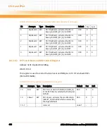
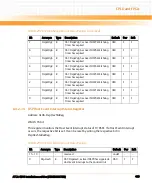
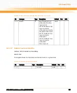
Table 8-202 DSP Watchdog Interrupt Status Register

Bit

Acronym

Type

Description

Default

Pwr

Soft

15...10

-

-

reserved

undef

-

-

9

DspWdg9

R

0b1: DspWdg9, active if DSP9 Watchdog 
Timer has expired

0b0

F

F

8

DspWdg8

R

0b1: DspWdg8, active if DSP8 Watchdog 
Timer has expired

0b0

F

F

Summary of Contents for ATCA-8310

Page 1: ...Embedded Computing for Business Critical ContinuityTM ATCA 8310 Installation and Use P N 6806800M72D March 2012 ...

Page 2: ...f without obligation of Emerson Network Power Embedded Computing to notify any person of such revision or changes Electronic versions of this material may be read online downloaded for personal use or referenced in another document as a URL to a Emerson Network Power Embedded Computing website The text itself may not be published commercially in print or electronic form edited translated or otherw...

Page 3: ...2 2 2 1 Environmental Requirements 42 2 2 2 Power Requirements 45 2 3 Blade Layout 47 2 4 Switch Settings 48 2 5 Installing and Removing the Blade 49 2 5 1 Installing the Blade 49 2 5 2 Removing the Blade 52 3 Controls Indicators and Connectors 55 3 1 Face Plate 55 3 1 1 LEDs 56 3 1 2 Keys 58 3 1 3 Connectors 59 3 2 Onboard Connectors 59 3 3 ATCA Backplane Connectors 59 3 4 Connector Pin Definitio...

Page 4: ... 2 1 9 I2C Interface 76 4 3 General Purpose Processor GPP 78 4 3 1 Intel x86 CPU 78 4 3 1 1 Thermal Monitor 79 4 3 1 2 Chipset Connection 79 4 3 1 3 GPP System Memory 79 4 3 2 Mobile Intel 5 Series Chipset 79 4 3 2 1 PCI Express Interface of the Ibex Peak 79 4 3 2 2 Ibex Peak Display 80 4 3 2 3 Ibex Peak LPC 80 4 3 2 4 Ibex Peak SPI 80 4 3 2 5 Ibex Peak SATA 80 4 3 2 6 Ibex Peak USB 80 4 3 2 7 GPP...

Page 5: ...anine Card Identifier 88 4 5 Ethernet Network ETH 89 4 5 1 Ethernet Network Overview 90 4 5 2 ETH Switch Unit 90 4 5 2 1 Ethernet Switch Device 90 4 5 2 2 Switch management 90 4 5 2 3 PHY connection 90 4 5 3 ATCA Fabric Interface 91 4 5 4 ATCA Base Interface and SOL 91 4 5 4 1 Serial over LAN 91 4 6 Timing Synchronization TS 91 4 6 1 Oscillator 95 4 7 Glue Logic FPGA 96 4 7 1 SPI System Overview 9...

Page 6: ...1 5 3 2 Advanced Menu 113 5 3 2 1 PCI Subsystem Sub menu 115 5 3 2 2 ACPI Settings 116 5 3 2 3 Trusted Computing 117 5 3 2 4 S5 RTC Wake Settings 118 5 3 2 5 CPU Configuration 119 5 3 2 6 ME Configuration 122 5 3 2 7 Thermal Configuration 123 5 3 2 8 Port 80h 127 5 3 2 9 TDT Configurations 128 5 3 2 10 USB Configurations 129 5 3 2 11 AMT Configuration 130 5 3 2 12 Super IO Configuration 131 5 3 2 ...

Page 7: ... 1 1 Memory Map 163 6 2 1 2 Environment Variables 164 6 2 1 3 Network interfaces 171 6 2 1 4 GPP Control 171 6 2 1 5 Firmware Update 174 6 2 1 6 FPGA Logic Operations 174 6 2 1 7 IPMI Interface 176 6 2 1 8 Application Boot 180 6 2 1 9 Default Boot Sequences 185 6 2 1 10 Broadcom Switch Configuration 186 6 2 1 11 Memory Initialization 190 6 2 1 12 SRIO Initialization 191 6 2 1 13 Miscellaneous Comm...

Page 8: ... FRU OEM Records 222 7 9 Reset Domains and FRU Activation Deactivation 224 7 10 U Boot Boot Configuration Parameters 225 7 11 Asynchronous Event Notification 227 7 12 Serial Line Selection 228 7 13 Built in Terminal Server 229 7 13 1 Evaluating the Version of the Telnet Server Firmware 230 7 13 2 Establishing a Telnet Session 231 7 14 Fail Safe Logic and Watchdog Support 232 7 14 1 SPP BMC Watchdo...

Page 9: ...Watchdog 258 8 1 5 2 IPMC IRQ 259 8 1 5 3 FPGA Configuration Logic 259 8 1 5 4 CPLD Serial Redirection 260 8 1 5 5 IPMC SPI Interfaces 261 8 1 5 6 FPGA SPI Interface 261 8 2 Glue Logic FPGA 261 8 2 1 Glue Logic FPGA Architectural Overview 262 8 2 1 1 Unit Description 263 8 2 2 Registers 264 8 2 2 1 Register Decoding 265 8 2 2 2 Glue Logic FPGA Register Mapping 291 8 2 2 3 Glue Logic FPGA Register ...

Page 10: ...nerator Block TstPatGenBlk 386 8 4 2 3 TSIP Interface Test Pattern Comparator Block TstPatCmpBlk 389 8 4 2 4 TSIP to Serializer Converter Block Tsip2SerBlk 393 8 4 2 5 Deserializer to TSIP Allocater Block Des2TsipBlk 396 8 4 2 6 DSP Reset and NMI Control Block DspResNmiCtrlBlk 402 8 4 2 7 DSP Status and Interrupt Block DspStaIntBlk 406 8 4 2 8 DMC Power Supply Control Block DmcPwrCtrlBlk 415 8 4 2...

Page 11: ...llation and Use 6806800M72D 11 A Replacing the Battery 439 A 1 Replacing the Battery 439 B Related Documentation 443 B 1 Emerson Network Power Embedded Computing Documents 443 Safety Notes 445 Sicherheitshinweise 449 Index 455 ...

Page 12: ...ATCA 8310 Installation and Use 6806800M72D Contents 12 Contents Contents ...

Page 13: ... 3 10 Serial Connector Pinout 68 Table 3 11 USB Connector Pinout 69 Table 4 1 SPI Chip Select Assignment 73 Table 4 2 P4080 I2C Bus Assignment 76 Table 4 3 PCI Express Interface of the Ibex Peak 79 Table 4 4 SMBus Address Map 81 Table 4 5 BASE_ID 87 Table 4 6 MOD_ID 87 Table 4 7 DMCx_ID 88 Table 4 8 ACS8520 Frequencies 91 Table 4 9 Resets 100 Table 5 1 Aptio Navigation 109 Table 5 2 Menu Descripti...

Page 14: ...l Port Console Redirection Field Description 134 Table 5 24 Console Redirection Settings 135 Table 5 25 Network Stack Field Description 137 Table 5 26 Chipset Menu Field Description 138 Table 5 27 North Bridge Configuration 139 Table 5 28 Common North Bridge Control Field Description 140 Table 5 29 PEG Port Configuration 141 Table 5 30 South Bridge Configuration 142 Table 5 31 Ibexpeak Options Fie...

Page 15: ... Table 7 4 Emerson ECC MAC Address Record 222 Table 7 5 Emerson ECC MAC Address Descriptor 223 Table 7 6 Interface Type Assignments 223 Table 7 7 IPMC Boot Parameter Storage Format 227 Table 7 8 TS Channel Information 230 Table 7 9 Emerson OEM Commands 237 Table 7 10 Set Serial Output Command 238 Table 7 11 Serial Output Selector Assignments 239 Table 7 12 Get Serial Output Command 240 Table 7 13 ...

Page 16: ...ster 257 Table 8 24 RTM FPGA device 1 force golden image or reload image Register 257 Table 8 25 RTM FPGA device 2 force golden image or reload image Register 257 Table 8 26 Register Default 264 Table 8 27 Register Access Type 264 Table 8 28 Byte Register Layout 265 Table 8 29 Word Register Layout 265 Table 8 30 LPC I O Register Map Overview 266 Table 8 31 POST Code Register 267 Table 8 32 Super I...

Page 17: ...egister LSR 285 Table 8 60 Modem Status Register MSR 288 Table 8 61 Scratch Register SCR 290 Table 8 62 Divisor Latch LSB Register DLL if DLAB 1 291 Table 8 63 Divisor Latch MSB Register DLM if DLAB 1 291 Table 8 64 Glue FPGA Register Overview 292 Table 8 65 Glue Logic FPGA Module Identification 294 Table 8 66 Glue Logic FPGA Code Version 295 Table 8 67 Serial Line Routing Register 295 Table 8 68 ...

Page 18: ...ailbox Output Registers 315 Table 8 98 SPP Mailbox Output Registers 315 Table 8 99 GPP Mailbox Input Registers 315 Table 8 100 SPP Mailbox Input Registers 315 Table 8 101 SPP Page Pointer 1 to Shared Memory 316 Table 8 102 GPP Page Pointer 1 to Shared Memory 316 Table 8 103 SPP Page Pointer 2 to Shared Memory 316 Table 8 104 GPP Page Pointer 2 to Shared Memory 316 Table 8 105 Semaphore Registers 3...

Page 19: ...rs 328 Table 8 133 Fault Event Status Register 329 Table 8 134 Fault Event Enable Register 330 Table 8 135 Software Fault Event 1 Register 332 Table 8 136 Software Fault Event 2 Register 332 Table 8 137 Software Fault Event 3Register 332 Table 8 138 Software Fault Event 4 Register 332 Table 8 139 SPP Interrupt Group Status Registers 333 Table 8 140 Cascade Interrupt Status Register 334 Table 8 141...

Page 20: ...ble 8 170 Terminal Server SPI Control Register 352 Table 8 171 BIOS Interrupt Mapping 356 Table 8 172 SPP Interrupt Routing 356 Table 8 173 GPP Serial Redirection Modes 366 Table 8 174 Logic DSP FPGA Register Overview 373 Table 8 175 SerDesPreselect Register 386 Table 8 176 Test Pattern Generator Link and Timeslot Register 387 Table 8 177 Test Pattern Generator Data Register 387 Table 8 178 Test P...

Page 21: ... Interrupt Status Reset Register 410 Table 8 205 DSP Host Event Interrupt Status Reset Register 412 Table 8 206 DSP Watchdog Interrupt Status Mask Register 413 Table 8 207 DSP Host Event Interrupt Status Mask Register 414 Table 8 208 DMC Power Supply Monitor Register 415 Table 8 209 Soft Reset Register 417 Table 8 210 Synchronization and Error Monitor Register 417 Table 8 211 Synchronization and E...

Page 22: ...Table 8 225 Test Mode Control Register 428 Table 8 226 Test Read Val Register 429 Table 8 227 I2C Bit Bang Register 430 Table 8 228 MDIO Bit Bang Register 432 Table 8 229 DSP FPGA debug LEDs 437 Table B 1 Emerson Network Power Embedded Computing Publications 443 ...

Page 23: ...hernet Overview 89 Figure 4 7 Telco Clock Structure 93 Figure 4 8 CLK1 CLK2 CLK3 Clock Structure 94 Figure 4 9 Telco Clock Structure Continued 95 Figure 4 10 Glue Logic FPGA Overview 96 Figure 4 11 SPI Overview 98 Figure 4 12 IPMC MMC block diagram of the ATCA 8310 99 Figure 5 1 Main Menu 108 Figure 5 2 Main Menu 110 Figure 5 3 Platform Information 111 Figure 5 4 Advanced Menu 113 Figure 5 5 PCI S...

Page 24: ...figuration 146 Figure 5 33 PCI Express Configuration 148 Figure 5 34 PCI to PCI Bridge 149 Figure 5 35 Boot Menu 150 Figure 5 36 Security Menu 151 Figure 5 37 Save Menu 152 Figure 7 1 IPMC MMC block diagram of the ATCA 8310 203 Figure 7 2 Firmware Architecture 205 Figure 7 3 IPMC Boot Parameter Storage Configuration Flow 226 Figure 7 4 COM 0 and IPMC Serial Line Selection 228 Figure 7 5 Com 1 Seri...

Page 25: ...800M72D 25 Figure 8 10 FPGA GPP Serial Redirection 366 Figure 8 11 SPP COM1 Serial Redirection 368 Figure 8 12 Dsp Fpga Overview 370 Figure 8 13 Logic blocks overview 434 Figure 8 14 122 912μs SERDES frame 435 Figure A 1 Location of Onboard Battery 439 ...

Page 26: ...ATCA 8310 Installation and Use 6806800M72D 26 List of Figures ...

Page 27: ...e z Hardware Preparation and Installation on page 41 outlines the installation requirements hardware accessories switch settings installation and removal procedures z Controls Indicators and Connectors on page 55 describes external interfaces of the blade This includes connectors and LEDs z Functional Description on page 71 describes the functional blocks of the blade in detail This includes a blo...

Page 28: ...t CPU Central Processing Unit DDR Dual Data Rate type of SDRAM DDR3 Double Data Rate 3 synchronous dynamic random access memory SDRAM is the name of the new DDR memory standard that is being developed as the successor to DDR2 SDRAM DFM Design for Manufacturability DFT Design for Test DMA Direct Memory Access DRAM Dynamic Random Access Memory ECC Error Correction Code EEPROM Electrically Erasable P...

Page 29: ...anagement Bus IPMB L The IPMB connecting the carrier IPMC to the AMC module MMC Intelligent Platform Management Controller IPMI Intelligent Platform Management Interface ITP In Target Probe JTAG Joint Test Action Group test interface for digital logic circuits L2 Level 2 as in L2 Cache LAN Local Area Network LED Light emitting Diode LFM Linear Feet per Minute LPC Low Pin Count LVDS Low Voltage Dif...

Page 30: ...vice OS Operating System PCB Printed Circuit Board PCH Platform Controller Hub PCI E PCI Express PHY Physical layer device for Ethernet PICMG PCI Industrial Computer Manufacturers Group PLL Phase Locked Loop POST Power on Self Test PP Payload Power PRD Product Requirements Document RC Root Complex RoHS Restriction of Hazardous Substances RS232 Recommended Standard 232C interface standard for seria...

Page 31: ...le Data SMBus System Management Bus SMI System Management Interrupt SODIMM Small Outline Dual in line Memory Module SPD Serial Presence Detect TBD To be decided TCP Transmission Control Protocol TDP Thermal Design Power Tx Transmit line of a duplex serial communication interface UART Universal Asynchronous Receiver Transmitter UDP User Datagram Protocol USB Universal Serial Bus Abbreviation Defini...

Page 32: ...on screenoutputandcoderelatedelements or commands in body text Courier Bold Used to characterize user input and to separate it from system output Reference Used for references and for table and figure descriptions File Exit Notation for selecting a submenu text Notation for variables and keys text Notation for software buttons to click on the screen and parameter description Repeated item for exam...

Page 33: ...property damage message No danger encountered Pay attention to important information Notation Description Part Number Publication Date Description 6806800M72A October 2011 First version 6806800M72B October 2011 Updated Figure Serial Number Location on page 39 and deleted Chapter 3 1 Mechanical Layout 6806800M72C December 2011 Updated Table 4 8 6806800M72D March 2012 Added Notice in Installation on...

Page 34: ...ATCA 8310 Installation and Use 6806800M72D About this Manual 34 About this Manual ...

Page 35: ... P4080 for local setup call control and load balancing z Build option for Intel Arrandale ECC CPU with on board mass storage for localized call agent z 10G fabric interface with multiple non blocking internal data paths z Clock termination and sync z Architecture ready for next generation TNETV3030 DSP z External Connectivity Wireline I O RTM different RTM 8x OC 3 or 2 x OC 12 line terminations fo...

Page 36: ...A C22 2 No 60950 1 Legal safety requirements CISPR 22 CISPR 24 EN 55022 EN 55024 FCC Part 15 Industry Canada ICES 003 VCCI Japan AS NZS CISPR 22 EN 300 386 NEBS Standard GR 1089 CORE EMC requirements legal on system level predefined Emerson system NEBS Standard GR 63 CORE ETSI EN 300019 series Environmental requirements PICMG 3 0 Defines mechanics blade dimensions power distribution power and data...

Page 37: ...d and Logic Ground logic signal return have to be connected The connection may be implemented inside the shelf for example at the backplane or the shelf has to provide a possibility to lead Logic Ground out of the shelf for external connection to Central Office Ground For further information refer to Telcordia GR 1089 CORE section 9 8 2 requirement R9 14 z The product has been designed to meet the...

Page 38: ...Introduction ATCA 8310 Installation and Use 6806800M72D 38 Figure 1 1 Declaration of Conformity ...

Page 39: ...lade smechanicaldata suchasdimensionsand weight 1 4 Product Identification The following figure show the location of the serial number labels Table 1 2 Mechanical Data Feature Value Dimensions width x height x depth 30 mm x 351 mm x 312 mm 8U form factor Weight of blade 2 5kg Figure 1 2 Serial Number Location Serial Number ...

Page 40: ...be created on customer request ATCA 8310 IA T5 ATCA DSP blade with X86 processor 5x TMS320TCI6486 DSP installed and 2 free mezzanine sites ATCA 8310 IA T10 ATCA DSP blade with X86 processor 10x TMS320TCI6486 DSP installed and 2 free mezzanine sites ATCA 8310 IA T20 ATCA DSP blade with X86 processor 20x TMS320TCI6486 DSP BOM will be created on customer request ATCA 8310 IA T30 ATCA DSP blade with X...

Page 41: ...nd report any damage or differences to the customer service 3 Remove the desiccant bag shipped together with the blade and dispose of it according to your country s legislation Damage of Circuits Electrostatic discharge and incorrect blade installation and removal can damage circuits or shorten their life Before touching the blade or electronic components make sure that you are working in an ESD s...

Page 42: ... requirements of the blade may be further limited down due to installed accessories such as hard disks or PMC modules with more restrictive environmental requirements z Operating temperatures refer to the temperature of the air circulating around the blade and not to the actual component temperature Blade Damage Blade Surface High humidity and condensation on the blade surface causes short circuit...

Page 43: ...ion according to NEBS Standard GR 63 CORE 40 ºC 40 F to 70 ºC 158 F Airflow The blade is designed to operate in a chassis that provides B4 cooling per CP TA Temp change 0 25 ºC min according to NEBS Standard GR 63 CORE 0 25 ºC min Rel humidity 5 to 90 non condensing 5 to 95 non condensing Vibration 20 to 2000Hz 0 1 g from 5 to 100 Hz Rack Level according to NEBS Standard GR 63 CORE 5 20 Hz at 0 01...

Page 44: ...R1595 R1596 F4 F4 C961 C961 C2012 C2012 P47 P47 R1597 C2359 C2359 C2360 C2360 R1844 C2401 C2401 C1100 C1100 C1099 C1099 C1197 C1197 C1198 C1198 C2337 C2337 C2338 C2338 C2336 C2336 ZSSD2 5 4 8 1 R 3 8 4 2 C SW2 SW2 F7 F6 Q7 U77 U77 U78 U78 C1192 C1189 J77 R282 C2457 R285 R286 F9 MH1 F8 C1068 C1077 C1077 U13 U13 C1092 C1093 C1194 C1195 C1187 C1196 R1616 R1600 R279 R281 J38 C828 C827 C860 E47 C1075 C...

Page 45: ...for a safety extra low voltage SELV under normal operating conditions and which is not subject to over voltages from telecommunication networks Table 2 2 Power Requirements Characteristic Value Rated Voltage 48 VDC to 60 VDC US and Canada 48 VDC Operating Voltage 40 VDC to 72 VDC US and Canada 40 VDC to 60 VDC Max power consumption ATCA 8310 base board 200W ATCA 8310 Mezzanines up to two provided ...

Page 46: ... simultaneously exercising as many functions and interfaces as possible This includes a particular load software provided by Intel designed to stress the processors to reach their theoretical maximum power specification Any difference in the system configuration or the software executed by the processors may affect the actual power dissipation Depending on the actual operating configuration and co...

Page 47: ...rdware Preparation and Installation ATCA 8310 Installation and Use 6806800M72D 47 2 3 Blade Layout The following figure shows the location of components on the ATCA 8310 Figure 2 2 ATCA 8310 Blade Layout ...

Page 48: ...ns and may cause the blade to malfunction if their setting is changed Therefore donotchange settings ofswitches marked as Reserved The setting ofswitches which are not marked as Reserved has to be checked and changed before blade installation Blade Damage Setting resetting the switches during operation can cause blade damage Therefore check and change switch settings before you install the blade A...

Page 49: ... slot 2 5 1 Installing the Blade To install the blade into an AdvancedTCA shelf proceed as follows Damage of Circuits Electrostatic discharge and incorrect blade installation and removal can damage circuits or shorten their life Before touching the blade or electronic components make sure that you are working in an ESD safe environment Blade Malfunctioning Incorrect blade installation and removal ...

Page 50: ... and bottom ejector handles are in the outward position by squeezing the lever and the latch together 2 Insert blade into the shelf by placing the top and bottom edges of the blade in the card guides of the shelf Ensure that the guiding module of shelf and blade are aligned properly 3 Apply equal and steady pressure to the blade to carefully slide the blade into the shelf until you feel resistance...

Page 51: ...ompletely installed the blue LED starts to blink This indicates that the blade announces its presence to the shelf management controller 6 Wait until the blue LED is switched off then tighten the face plate screws which secure the blade to the shelf The switched off blue LED indicates that the blade s payload has been powered up and that the blade is active 7 Connect cables to the face plate if ap...

Page 52: ...face plate Do not rotate the handle fully outward The blue LED blinks indicating that the blade power down process is ongoing 2 Wait until the blue LED is illuminated permanently then unlatch the upper handle and rotate both handles fully outward Damage of Circuits Electrostatic discharge and incorrect blade installation and removal can damage circuits or shorten their life Before touching the bla...

Page 53: ...e plate cables if applicable 4 Unfasten the screws of the face plate until the blade is detached from the shelf 5 Remove the blade from the shelf Data Loss Removing the blade with the blue LED still blinking causes data loss Wait until the blue LED is permanently illuminated before removing the blade ...

Page 54: ...Hardware Preparation and Installation ATCA 8310 Installation and Use 6806800M72D 54 ...

Page 55: ...3 ATCA 8310 Installation and Use 6806800M72D 55 Controls Indicators and Connectors 3 1 Face Plate The following figure illustrates the connectors keys and LEDs available at the face plate Figure 3 1 Face Plate ...

Page 56: ...ls Indicators and Connectors ATCA 8310 Installation and Use 6806800M72D 56 3 1 1 LEDs The following figure illustrates all LEDs available at the face plate Figure 3 2 Location of Face Plate LEDs Link Activity ...

Page 57: ...this LED indicates the payload power status both in the early power state and the normal blade operation OFF Payload power is disabled Note This LED is multicolored red green yellow and is programmable by IPMC ATN Amber This LED is controlled by higher layer software such as middle ware or applications ETH Status LEDs The Ethernet connector provides two status LEDs Link upper Green Link is availab...

Page 58: ...U State Machine During blade installation Permanently blue On board IPMC powers up Blinking blue Blade communicates with shelf manager OFF Blade is active During blade removal Blinking blue Blade notifies shelf manager of its desire to deactivate Permanently blue Blade is ready to be extracted Table 3 1 Face Plate LEDs continued LED Description Figure 3 3 Location of Face Plate Reset Key You canno...

Page 59: ... s connected to FPGA for BASE IF and Faceplate IF Link Control FPGA control Recessed reset button 3 2 Onboard Connectors The blade provides the following on board connectors z 2x Module Connector for DSP Mezzanine Card 3 3 ATCA Backplane Connectors The ATCA specification defines Zone 3 for user input output signals On ATCA 8310 ATCA Zone 3 Type A connector direct connect to RTM are used The same c...

Page 60: ...Controls Indicators and Connectors ATCA 8310 Installation and Use 6806800M72D 60 Figure 3 4 Location of AdvancedTCA Connectors ...

Page 61: ...ed Reserved Reserved Reserved Reserved Reserved Reserved 7 Reserved NC NC NC Reserved Reserved Reserved Reserved 8 Reserved Reserved Reserved Reserved Reserved Reserved Reserved Reserved 9 NC NC NC NC NC NC NC NC 10 NC NC NC NC NC NC NC NC Table 3 3 Zone 2 P23 Pin Assignment P23 Row Interface Col AB Col CD Col EF Col GH 1 Fabric Ch1 FAB1_TX2 FAB1_TX2 FAB1_RX2 FAB1_RX2 FAB1_TX3 FAB1_TX3 FAB1_RX3 FA...

Page 62: ..._RTM RXD SERIAL_RTM TXD NC NC NC NC PS1_N RTM_PWRGD 2 NC NC NC TRACKDWN_ VP RTM NC RTM2 FORCE GOLDEN RTM1 FORCE GOLDEN RTM0 FORCE GOLDEN 3 SPI_MOSI NC SPI_MISO NC SPI_CLK SPI_CLK1 SPI_CS_N NC 4 CLK_T3 Bits NC HEALTHY OUT CONF_CRC ERR RTM_ACTIVE OUT FPGA_DONE FPGA_INTI_N FPGA_PROG_N 5 NC NC NC NC NC NC NC NC 6 PCIE_RX0 PCIE_RX0 PCIE_TX0 PCIE_TX0 PCIE_RX1 PCIE_RX1 PCIE_TX1 PCIE_TX1 7 100MHz_PCIE CLK...

Page 63: ...TX 7 DMC1_TSIP0 RX DMC1_TSIP0 RX DMC1_TSIP0 TX DMC1_TSIP0 TX DMC1_TSIP1 RX DMC1_TSIP1 RX DMC1_TSIP1 TX DMC1_TSIP1 TX 8 DMC2_TSIP0 RX DMC2_TSIP0 RX DMC2_TSIP0 TX DMC2_TSIP0 TX DMC2_TSIP1 RX DMC2_TSIP1 RX DMC2_TSIP1 TX DMC2_TSIP1 TX 9 RTM2_TSIP_C LK RTM2_TSIP_C LK RTM1_TSIP_C LK RTM1_TSIP_C LK RTM_TSIP_CL K RTM_TSIP_CL K CLK_166Hz NC 10 VP12 NC NC NC NC NC VP12 VP12 Table 3 6 Zone 3 P32 Pin Assignme...

Page 64: ...2 Pin Assignment P32 Row Col AB Col CD Col EF Col GH Table 3 7 DMC Mezzanine Connector Pinout Signal Pin Pin Signal SRIO0_TX 1 2 SRIO1_TX SRIO0_TX 3 4 SRIO1_TX GND 5 6 GND SRIO_CLK 7 8 SRIO1_RX SRIO_CLK 9 10 SRIO1_RX GND 11 12 GND SRIO0_RX 13 14 NC SRIO0_RX 15 16 NC GND 17 18 NC SG1_TX 19 20 SG12_TX SG1_TX 21 22 SG12_TX SG1_RX 23 24 SG12_RX SG1_RX 25 26 SG12_RX VP12 27 28 VP12 SG2_TX 29 30 SG11_TX...

Page 65: ... 50 SG9_TX SG4_TX 51 52 SG9_TX SG4_RX 53 54 SG9_RX SG4_RX 55 56 SG9_RX VP12 57 58 VP12 SG5_TX 59 60 SG8_TX SG5_TX 61 62 SG8_TX SG5_RX 63 64 SG8_RX SG5_RX 65 66 SG8_RX VP12 67 68 VP12 SG6_TX 69 70 SG7_TX SG6_TX 71 72 SG7_TX SG6_RX 73 74 SG7_RX SG6_RX 75 76 SG7_RX GND 77 78 NC SG13_TX 79 80 NC SG13_TX 81 82 NC SG13_RX 83 84 NC SG13_RX 85 86 NC GND 87 88 NC Table 3 7 DMC Mezzanine Connector Pinout co...

Page 66: ...N 109 110 HOUT_DSP_N DMC_PWRGD 111 112 CONF_CRC_ERR DMC_FPGA_PROG_N 113 114 FPGA_INIT_N JTAG_TRST_N 115 116 FPGA_DONE JTAG_TDO 117 118 FPGA_JTAG_TDO JTAG_TDI 119 120 FPGA_JTAG_TDI JTAG_TCK 121 122 FPGA_JTAG_TCK TAG_TMS 123 124 FPGA_JTAG_TMS SOI_MOSI 125 126 V3P3_MGMT SPI_MISO 127 128 I2C_SDA_BUF SPI_CLK 129 130 I2C_SCL_BUF SPI_CS_N 131 132 BRD_PWROK V3P3 133 134 V3P3 TSIP_CLK 135 136 CLK_8K TSIP_C...

Page 67: ...0 TSIP0_TX V1P2 151 152 V1P2 Table 3 7 DMC Mezzanine Connector Pinout continued Signal Pin Pin Signal The pinoutsonTable3 7on page64applies tobothmezzanineconnectors Thesignalnames are then named DMC1 DMC2 Table 3 8 VGA Connector Pinout Pin Signal Pin Signal 1 CRT RED 9 VP5 2 CRT GREEN 10 GND 3 CRT BLUE 11 NC 4 NC 12 DDC DATA 5 GND 13 CRT HSYNC 6 GND 14 CRT VSYNC 7 GND 15 DDC CLK 8 GND ...

Page 68: ...d Use 6806800M72D 68 3 4 5 Ethernet Connector 3 4 6 Serial Connector Table 3 9 Ethernet Connector Pinout Pin Signal 1 TRD0 2 TRD0 3 TRD1 4 TRD2 5 TRD2 6 TRD1 7 TRD3 8 TRD3 Table 3 10 Serial Connector Pinout Pin Signal 1 NC 2 NC 3 TXD 4 GND 5 GND 6 RXD 7 NC 8 NC ...

Page 69: ...Controls Indicators and Connectors ATCA 8310 Installation and Use 6806800M72D 69 3 4 7 USB Connector Table 3 11 USB Connector Pinout Pin Signal 1 VP5 2 USB 3 USB 4 GND ...

Page 70: ...Controls Indicators and Connectors ATCA 8310 Installation and Use 6806800M72D 70 ...

Page 71: ...FPGA BCM 56624 Tsi 572 PHY 1 GbE XAUI PCIe n PCI 33 SRIO n Local Bus Arendale IBEX Peak Zone 2 Zone 3 PHY 82571 CLK store TSIP SPI USB SPI Local Bus PCIe 1 rear 1 SRIO 1 SRIO 4 SRIO 1 SRIO BI BI FI FI QPI BI BI 30 TSIP 2 GbE 30 GbE PHY SGMII ACS 8520 CLK3AB CLK1 2AB TSIP LREFCLK1 2 REFCLK 0 2 T3 T4 MFrSync FrSync 8kHz 19 44MHz CLK166 UC CLK MSSYNC 8kHz UC 2 ESSI 2 RX MS CNTR PCIe 4 GbE PHY store S...

Page 72: ...z Setting up and controlling the switch z Running certain applications as required e g IP SEC The Freescale P4080 processor is used for these purposes Figure 4 2 Service Processor Overview Zone2 UC 1 XAUI Glue FPGA SPI Flash boot 2 PCIe FPRL P4080 BCM 56624 2 PCIe Zone3 1 SRIO Tsi 572 Local BUS USB Flash SPI Interface USB Dual Channel DDR3 ACS 8520 USB COM I2C0 I2C1 RTC IPMI COM1 2 USB PHY 2 SGMII...

Page 73: ...onnected to the FPGA as spare signals LCS4 7 are not used 4 2 1 2 SPI Interface The Freescale P4080 includes a full duplex four wire SPI interface The SPI interface can support up to four separate SPI devices The P4080 SPI interface is routed to the ACS8520B linecard PLL and to the SPI boot Flashes The following table shows the P4080 chip select assignments for the SPI devices 4 2 1 2 1 Boot Flash...

Page 74: ...chanism is described in the software specification The principal is to store the information which device was used to boot from and keep that device protected The redundant device can then be upgraded as needed In case of an IPMC firmware upgrade the BOOT_SELECT signal stays unchanged Besides others this signal is latched by a latch buffer to ensure that its state doesn t change when the IPMC rese...

Page 75: ...s Configuration The Freescale P4080 provides 18 Serdes lanes that can be mapped to different IO Interfaces The following interfaces are required z 2x PCI Express one to the RTM one to the switch z 1x SRIO z 1x XAUI to the switch z 2x SGMII to the switch 4 2 1 5 Freescale P4080 PCI Express The Freescale P4080 provides three PCI Express 2 0 controllers running up to 5 GHz Two of them are used on the...

Page 76: ... routed to the Glue Logic FPGA Only the TXD and RXD signals are used for this interface The serial port parameters for this port are 9600 baud 8 data bits no parity 1 stop bit 4 2 1 9 I2C Interface The Freescale P4080 includes a dual I2C controller Both open drain two wire interfaces provide multiple master and master slave I2C mode support I2C bus 0 is used to connect to a boot sequencer memory a...

Page 77: ...ime clock calendar provides seconds minutes hours day date month and year information The end of the month date is automatically adjusted for months with fewer than 31 days including corrections for leap year up to the year 2100 The clock operates in either the 24hr or 12hr formatwith an AM PM indicator The timekeeping supply current for this device is max 0 63uA Battery backup is provided with on...

Page 78: ... 3 1 Intel x86 CPU The Arrandale ECC consistsoftwo dies TheCPU core whichisbased onthe Nehalem core and the Ironlake GMCH core which includes memory and graphic controller Figure 4 4 Block Diagram of the GPP Part Arrandale ECC IBEX PEAK Mobile QM57 Dual Channel DDR3 800 1066 MT s IMVP 6 5 XDP FDI DMI x4 82574 GbE LAN Glue Logic FPGA SPI Flash SPI Flash CRT VGA 2x USB 1x SATA SPI LPC SMBUS PCIe Por...

Page 79: ...s Unbuffered DDR3 memory with one DIMM slot per channel is supported The speed grade is 800 1066 The ATCA 8310 provides two very Low Profile VLP Mini DIMM sockets to install off the shelf DIMM modules Different DIMM types must not be used at the same time DIMM module height is restricted 4 3 2 Mobile Intel 5 Series Chipset The Mobile Intel 5 Series Chipset is available in different flavours Two of...

Page 80: ...OT Flash choice and the BIOS update over IPMI will be implemented 4 3 2 5 Ibex Peak SATA SATA port 1 is routed to the onboard 1 8 SSD All other SATA Ports are not used on the ATCA 8310 4 3 2 6 Ibex Peak USB USB port 1 and 2 are routed to the front panel 4 3 2 7 GPP System Management Bus SMBus The Ibex Peak contains a SMBus Host interface that allows the processor to communicate with SMBus slaves T...

Page 81: ... backup 4 3 3 GPP Ethernet Connectivity Two Ethernet connections are provided from the GPP to the switch For other purposes one Ethernet interface is available on the front panel Table 4 4 SMBus Address Map Device Name Device Type Location SM BUS Address SPD EEPROM 24C02 DIMMA 0xA0 SPD EEPROM 24C02 DIMMB 0xA4 Thermal Sensor DIMMA 0x30 SPD EEPROM DIMMB 0x34 DDR3 VREF_D margening ISL90728 Base Board...

Page 82: ... 30 x TNETV3020 Tomahawk DSPs TNETV3020 The DSPs are distributed between three modules each with 10 DSPs Module 0 is assembled on baseboard Module 1 and 2 are arranged on two mezzanine cards DSP MC1 and DSP MC2 Factory assembly options allow baseboard module configurations with 0 5 and 10 DSPs In total this gives options for 5 10 15 20 25 and 30 DSPs The DSP mezzanines are not hot swappable Howeve...

Page 83: ... via module connector 4 4 1 Digital Signal Processor The TNETV3020 device is a Texas Instruments fixed point voice over packet digital signal processor DSP targeting telephony infrastructure applications including voice over packet high density and medium density gateways wireless media gateways and remote access servers Figure 4 5 DSP Cluster Block Diagram DSP4 PHY 23 DSP3 DSP2 DDR2 PHY 01 DSP1 D...

Page 84: ...nterrupt event generation modes and a 16 bit multiplexed host port interface HPI16 4 4 1 1 DSP Configuration Following interfaces are not used and disable by strapping option z UTOPIA Interface z TSIP Interface 1 and 2 z EMAC Interface 1 The DSPs run with 500 MHz core clock 4 4 1 2 Boot Mode Selection The desired boot mode is selected by setting the four boot mode select pins BOOTMODE 3 0 which ar...

Page 85: ...consisting of a maximum of eight transmit data signals or links eight receive data signals or links two frame sync input signals and two serial clock inputs The TSIP module offers support for a maximum of 1024 timeslots for transmit and receive Typically 672 timeslots DS3 for transmit and receive are utilized on these links The TSIP module can be configured to use the frame sync signals and the se...

Page 86: ...e the PHY devices and read back PHY link information The BCM5482 offers an interface converter mode that supports RGMII to SGMII slave data conversion Each one of the PHY ports has a secondary SerDes that is used to perform conversion 4 4 6 DSP FPGA The DSP FPGA is the main control unit on the DSP cluster It controls all DSP functionality including TSIP interface to the RTM and the power sequencin...

Page 87: ... 4 4 8 2 Module Functional Identifier The Module Functional Identifier MOD_ID delivers information about the functionality of the DSP Mezzanine Card The MOD_ID is readable by the ModuleFunctionalIdReg Address 0xC6 of the DSP FPGA Table 4 5 BASE_ID BASE_ID 3 0 Description 0b1100 DSP FPGA on base board DMC0 0b1101 DSP FPGA on mezzanine card 1 DMC1 0b1110 DSP FPGA on mezzanine card 2 DMC2 0b1111 GLUE...

Page 88: ...ormation about the availability and type of DSP Mezzanine Cards and is used for power control requirements inside the CPLD The DMCx_ID of each module is readable by the status registers Address 0x02 0x03 of the Power Up CPLD Table 4 7 DMCx_ID DMCx_ID 3 0 Description 0b1111 DSP Mezzanine Card not available 0b1110 DSP Mezzanine Card available All others reserved ...

Page 89: ...h device is used This switch is configured by the service processor Figure 4 6 Ethernet Overview BCM 56624 DSP farm 0 onboard GPP CPU Zone3 Zone2 MCF 52232 UC 2 SGMII 2 SGMII BI BI 2 XAUI 6 SGMII XAUI ARTM SPP CPU XAUI 2 PCIe FPRL BCM 5482 5 Dual PHY SGMII to RGMII SGMII 2 SGMII DSP farm 1 module1 BCM 5482 5 Dual PHY SGMII to RGMII DSP farm 2 module2 BCM 5482 5 Dual PHY SGMII to RGMII 13 SGMII 13 ...

Page 90: ...the Freescale P4080 High end switching systems use the PCI express interfaces for setup configuration maintenance and management of the BCM56624 Switch In high end systems requiring the host CPU running routing protocol stacks PCI express bus is necessary for moving data packets to and from CPU For ATCA 8310 the BCM56624 provides switching between any on board Ethernet port and the backplane inter...

Page 91: ...se Interface of the ATCA 8310 is also provided by the Switching Unit Two SGMII lanes are connected to a MARVELL 88E6161 switch This switch has 1000B T ports to the Baseinterface Itisconfiguredat powerupviaserial prom which allowsfor immediate SOL after power up 4 5 4 1 Serial over LAN The serialoverLANfunctionalityisprovidedby aFreescalecontroller Thisdevice transformsup to two RS232 ports to Ethe...

Page 92: ... 25MHz FPGA to 8520 SYNC2K 2kHz T3 1 544 2 04 8MHz MFrSync 2kHz MultiFrameSync ACS8520 to Zone3 FrSync 8kHz FrameSync ACS8520 1x Zone3 3x DSP FPGA SBI_CLK 77 76MHz 1x Zone3 1x GlueLogic FPGA MVIP_CLK 16 384MHz 1x Zone3 RTM TSIP_CLK 32 768MHz 3x DSP FPGA 1x Zone3 RTM ETH_CLK_ OUT 25MHz Ethernet CLK output to Zone 3 T4 1 544 2 048 MHz To RTM Zone 3 DS3_CLK 34 44 51 MHz To RTM Zone 3 Table 4 8 ACS852...

Page 93: ... CMAC E2747 TO10 FrSync 8kHz T3 BITS I14 Semtech M1 REFCLK1 REFCLK2 CLK3B CLK3A CLK2A CLK1A CLK2B CLK1B I5 Semtech I7 Semtech I6 Semtech I8 Semtech SYNC_2 CLK1A CLK1B SYNC2K Semtech TO9 1 544 2 048MHz T4 TO6 DS3_CLK 12 283MHz I10 Semtech I9 Semtech S5 S6 TO1 6 48MHz 166 7Hz out Zone 3 BP Zone2 ADM Glue FPGA 166 7Hz MSSYNC diff 6 48M M2 RXCLK 1 RXCLK 2 RXCLK 3 RXCLK N 2 RXCLK N 1 RXCLK N TO11 MFrSy...

Page 94: ...A 8310 Installation and Use 6806800M72D 94 Figure 4 8 CLK1 CLK2 CLK3 Clock Structure CLK2A CLK2B CLK1A CLK1B ACS 8520B SYNC_2 CLK3A CLK3B Zone2 REFCLK1 REFCLK2 EN_CLK3B EN_CLK3A I9 I10 Sync2K I8 I7 I13 I12 I14 T3 BITS 8kHz I3 I4 ...

Page 95: ... stability is determined by the oscillator quality The following Oscillator is used CMACStratum 3 E2747 3 3V Figure 4 9 Telco Clock Structure Continued TO11 MFrSync 2kHz Zone3 TO10 FrSync 8kHz TO5 77 76MHz TO3 32 768MHz TO4 25MHz TO9 T4 1 544 2 048MHz TO1 6 48MHz TO6 DS3_CLK 34 44 51MHz ACS 8520B ADM I11 166 7Hz 166Hz 3x DSP FPGA 3x DSP FPGA TO2 16 384MHz TO2 16 384MHz TO7 RTM_CLK_TO7 ...

Page 96: ...lays SPP Local Bus Super IO Watchdog signals LPC Bus Interface COM 2 COM 1 IPMC LPC Bus GPP LPC Bus IPMC SERIRQ GPP SERIRQ GPP Interrupt Controller IPMC SPI Interface DMX 2 Interface DMX 1 Interface DMX Base Interface GPP Interrupt Signals SPP Watchdog Controller SPP Reset Controller SPP Interrupt Controller GPP SPP Shared Memory SPP Reset Signals SPP Watchdog Signals GPP Interrupt Signals CPLD SP...

Page 97: ...Register z GPP SPP Shared Memory z SPI Interface to update Glue FPGA Configuration Flash z Two Serial Interfaces COM1 and COM2 usable via Super IO mapping for GPP z Watchdog Controller for GPP and SPP z Reset Controller for GPP and SPP z Routing of internal and externals GPP Interrupts via SERIRQ protocol z Routing of internal and externals SPP Interrupts to SPP interrupt input signals z Interrupt...

Page 98: ...GA SPI Flash Config SPI Glue Logic FPGA DSP FPGA SPI Flash Config SPI DSP FPGA SPI Flash Config SPI SPI Bus SPI Bus SPI Bus SPI Flash Config SPI RTM FPGA base SPI Flash Config SPI SPI Bus TSI FPGA SPI Flash Config SPI PCIe RTM FPGA TSI XO SPI Flash Config SPI SPI Bus SPI Bus RTM RTM piggy pack Bussed internally ...

Page 99: ...ification Figure 4 12 IPMC MMC block diagram of the ATCA 8310 FRU Information Temperature Sensor Presence Sensor DSP Module FRU Information Temperature Sensor Presence Sensor DMC Module Renesas H8S 2166 IPMC I2 C IPMB 0 IPMB A IPMB B IPMB L ATMEGA 128 MMC at RTM Temperature Sensors ATCA 8310 FRU Information Power Interface Sensors Voltage Sensors System Event Log SEL I2 C FRU Information Temperatu...

Page 100: ...s signals are asserted CPU RESET is used to reset all internal registers state machines and caches of the processor The PCI_RST PLT_RST is used to reset all onboard PCI PCIe participants of all onboard PCI PCIe busses The P4080 is also reset by the PLT_RST signal and generates CPU RESET to the Nehalem EP processors 4 9 1 1 2 Warm Reset DuringaWarmResettheP4080assertstheINIT signalfor16processorclo...

Page 101: ...o the Glue Logic FPGA which propagates it to the PWROK input of the P4080 respecting the PWROK input min assertion of 99msec The DDR3 DIMMs are reset directly from the processors individually per memory channel and CPU during power up only according DDR specification 4 9 1 3 2 Software Controlled Reset Software is able to generate a Cold and a Warm reset Depending on the configuration 4 9 1 3 3 Fa...

Page 102: ... payload power of the ATCA 8310 carrier board is in a power cycle The IPMC drives the ENABLE signal active low as an input to the RTM AMC module Beside the IPMC reset an RTM module can be reset through Software via the PCI Express interface protocol Beside the IPMC also the reset controller inside the Glue Logic FPGA can control RESET the RTM In case of hot swap the RTM will be reset by the IPMC D...

Page 103: ...ed z btime booting start time z shelf atca shelf id z slot_p physical slot the board occupies in the shelf z slot_l logical slot the board occupies in the shelf z ea1 ethernet mac address 1 z ea2 ethernet mac address 2 z ea3 ethernet mac address 3 z clid dhcp client id z btorder boot order z bootwd boot watchdog 5 1 1 1 clid Parameter The clid parameter s value shall be used to fill in an UUID fie...

Page 104: ...sbhdd The boot option names shall be written one after another separated by commas without any blank spaces 5 1 1 3 bootwd Parameter The bootwd parameter s value shall be used as a timeout value of the GPP Watchdog realized in the Glue Logic FPGA of the ATCA 8310 board If the bootwd parameter is defined the Watchdog shall be started by the BIOS just before booting to control the boot process Take ...

Page 105: ...e list may be defined using the setup menu or by means of btorder Shared Memory Parameter The names of boot options starting with uefi imply UEFI aware bootable device All other boot option names imply bootable devices according to the BBS 5 1 3 Redirection of Console I O Redirection of I O to COM port makes it possible to control the ATCA 8310 in an embedded environment where no VGA terminal is p...

Page 106: ... reset the BIOS performs a self test POST which attempts to determine if further operation is possible and that the detected configuration is expected This process can complete normally or result in a warning or an error The boot process does not stop after a warning but displays a message on the primary display device If an error is detected the boot process is halted If possible a message is dis...

Page 107: ...able device CD DVD HDD Network During the boot process board information messages will be displayed e g Emerson ATCA 8310 BIOS Version 1 3 6a 06 29 2011 18 02 48 Reset Type cold reset Cpu Arrandale ECC Measured Cpu Freq 1995 MHz Total Memory 4096 MB DDR3 1067 MHz FPGA version 8310 1EW Boot Flash Selection 0x00 Boot parameters clid 00 00 65 cd 00 2b ff 01 01 ff ff ff ff ff ff ff ff 5 2 3 Initiating...

Page 108: ... Setup Utility The BIOS Setup Utility provides for an interactive user interface which allows to alter a variety of system options The current system settings are stored in the NVRAM located in the same SPI Flash containing the BIOS This section describes the operation of the utility by describing the various options available through a set of hierarchical menus The picture below shows the first i...

Page 109: ...wn The Up and Down arrow keys allow to select a sub menu or an item Plus Minus The Plus and Minus keys allow to change the field value of a particular setup item TAB The Tab key allows to select fields ESC The Esc key allows to exit the Aptio Setup without saving of any changes When you are in a sub menu Esc key allows to get to the upper level menu Fn Function n When any Function keys become avai...

Page 110: ...on USB Configuration AMT Configuration Super IO Configuration Serial Port Console Redirection Network Stack Chipset Chipset Compatibility ID Settings North Bridge Configuration South Bridge Configuration Boot Boot Mode Settings Boot Options Security Setup Administrator and User Password options HDD Security Configuration Save exit Save Discard Changes options Restore Defaults Boot Override Table 5...

Page 111: ...Core Version AMI BIOS Core Version Project Version BIOS Project Name and Version Total Memory Total amount of memory installed Platform Information Platform Information Sub Menu System Language System default language fur messages and Setup Utility System date Set the Date System Time Set the Time Access Level Administrator or User Figure 5 3 Platform Information ...

Page 112: ...r Processor Core Dual CPU Core SMT Simultaneous Multithreading supported QPI Frequency Transactions per second at communication between the CPU Cores as well as between the CPU and the Chipset Total Memory Total amount of installed memory with type and frequency Memory Slot0 Amount of memory and its type installed in the DIMM Slot 0 Memory Slot1 Amount of memory and its type installed in the DIMM ...

Page 113: ...ns Launch Storage OpROM Enable Disable Boot Option for Legacy Mass Storage Devices with Option ROM Use FPGA RTC Use or not the Glue Logic FPGA RTC for initialization of System Date and Time at startup PCI Subsystem Settings PCI Subsystem Sub Menu ACPI settings ACPI Sub Menu Trusted Computing Trusted Computing Sub Menu S5 RTC Wake Settings S5 RTC Wake Sub Menu ...

Page 114: ...Sub Menu Port 80h Port 80h Sub Menu TDT Configuration TDT Sub Menu USB Configuration USB Sub Menu AMT Configuration AMT Sub Menu Super IO Configuration Super IO Sub Menu Serial Port Console Redirection Console Redirection Sub Menu Network Stack Network Stack Sub Menu Table 5 5 Advanced Menu Field Description continued Field Sub Menus Options ...

Page 115: ...e specifies what PCI Option ROM to launch PCI Latency Timer Value to be programmed into PCI Latency Timer Register VGA Palette Snoop Enables or Disables VGA Palette Registers Snooping PERR Generation Enables or Disables PCI Device to Generate PERR SERR Generation Enables or Disables PCI Device to Generate SERR Relaxed Ordering Enables or Disables PCI Express Device Relaxed Ordering Extended Tag If...

Page 116: ...tem BIOS select the value Maximum Read Request Set Maximum Read Request Size of PCI Express Device or allow System BIOS select the value Automatic ASPM Automatically enable ASPM based on reported capabilities and known issues Extended Synch If ENABLED allows generation of Extended Synchronization patterns Table 5 6 PCI Subsystem Sub menu Field Description continued Field Description Figure 5 6 ACP...

Page 117: ...bility to Hibernate OS S4 Sleep State This option may not be effective with some OSs PTID Support PTID Support will be loaded if enabled ACPI Sleep State Select the highest ACPI sleep state the system will enter when the SUSPEND button is pressed S3 Video Repost On enabling Video Option ROM will be dispatched during S3 resume Native PCIE Enable PCI Express Native Support Enable Disable This featur...

Page 118: ... 6806800M72D 118 5 3 2 4 S5 RTC Wake Settings Table 5 8 Trusted Computing Field Description Field Description TPM SUPPORT Enables or Disables TPM support O S will not show TPM Reset of platform is required Figure 5 8 S5 RTC Wake Settings ...

Page 119: ...e or disable System wake on alarm event When enabled System will wake on the hr min sec specified Wake up hour select 0 23 For example enter 3 for 3am and 15 for 3pm Wake up minute 0 59 Wake up second 0 59 Wake system with Dyna mic Time Enable or disable System wake on alarm event When enabled System will wake on the current time Increase minute s Figure 5 9 CPU Configuration ...

Page 120: ... OS OS not optimized for Hyper Threading Technology Active Processor Core Number of cores to enable in each processor package Limit CPUID Maximum Disabled for Windows XP Hardware Prefetcher To turn on off the MLC streamer prefetcher Adjacent Cache Line P refetch To turn on off prefetching of adjacent cache lines Intel Virtualization When enabled a VMM can utilize the additional hardware capabiliti...

Page 121: ...on Intel R SpeedStep tm Allows more than two freq range to be supported Boot performance mo de Select the performance state that the BIOS will set before OS handoff Turbo Mode Enable processor Turbo Mode requires EMTTM enabled too Extreme Edition Enable Disable Extreme Edition support C states Enable Disable CPU Power management Allows CPU to go to C states when it s not 100 utilized ...

Page 122: ...U will switch to minimum speed when all cores enter C State CPU C6 report Enable Disable CPU C6 ACPI C3 report to OS Number of VID states Sets the number of states in the special VID table At least 2 states must be present Table 5 11 Power and Performance Field Description continued Field Description Figure 5 11 ME Configuration ...

Page 123: ...e 5 12 ME Configuration Field Description Field Description End Of POST Message Enable Disable End of POST message sent to ME Figure 5 12 Thermal Configuration Table 5 13 Thermal Configuration Field Description Field Description CPU Thermal Configuration CPU Thermal Configuration options ...

Page 124: ...telligent Power Sharing options DPPM Configuration DPPM Configuration options Table 5 13 Thermal Configuration Field Description continued Field Description Figure 5 13 CPU Thermal Configuration Table 5 14 CPU Thermal Configuration Field Description Field Description DTS If disabled EC will be used to read CPU temperature If enabled individual CPU core temperature will be read from CPU ...

Page 125: ...or2 Bi directional PROCHOT When a processor thermal sensor trips either core the PROCHOT will bedriven If bi direction isenabled externalagents candrive PROCHOT to throttle the processor ACPI 3 0 T States Enable Disable ACPI 3 0 T States Table 5 14 CPU Thermal Configuration Field Description continued Field Description Figure 5 14 Platform Thermal Configuration ...

Page 126: ...rottling the processor Passive TC1 Value This value sets the TC1 value for the ACPI Passive Cooling Formula Range 1 16 Passive TC2 Value This value sets the TC2 value for the ACPI Passive Cooling Formula Range 1 16 Passive TSP Value This item sets the TSP value for the ACPI Passive Cooling Formula It represents in tenths of a second how often the OS will read the temperature when passive cooling i...

Page 127: ... ATCA 8310 Installation and Use 6806800M72D 127 5 3 2 8 Port 80h Figure 5 15 Port 80h Table 5 16 Port 80h Field Description Field Description Port 80h Redirection Control where the Port 80h cycles are sent ...

Page 128: ...D 128 5 3 2 9 TDT Configurations Figure 5 16 TDT Configurations Table 5 17 TDT Configurations Field Description Field Description TDT Enable Disable TDT in BIOS for testing only TDT Recovery Set the number of times Recovery attempt will be allowed ...

Page 129: ...ted DISABLE option will keep USB devices available only for EFI applications EHCI Hand off This is a workaround for OSes without EHCI hand off support The EHCI ownership change should be claimed by EHCI driver Device Reset timeout USB mass storage device Start Unit command timeout Controller Timeout The time out value for Control bulk interrupt transfer EHCI Hand off This is a workaround for OSes ...

Page 130: ...Opticaldrivesareemulatedas CDROM drives with no media will be emulated according to a drive type Table 5 18 USB Configurations Field Description continued Field Description Figure 5 18 AMT Configuration Table 5 19 AMT Configuration Field Description Field Description Intel AMT SPI Protect Enable Disable Intel AMT SPI write protect Me FW Downgrade Enable Disable Me FW Downgrade function ...

Page 131: ...Update function Table 5 19 AMT Configuration Field Description continued Field Description Figure 5 19 Super IO Configuration Table 5 20 Super IO Configuration Field Description Field Description Serial Port 0 Configuration Set Parameters of Serial Port 0 COMA Serial Port 1 Configuration Set Parameters of Serial Port 1 COMB ...

Page 132: ...2 12 1 Serial Port 0 Configuration Figure 5 20 Serial Port 0 Configuration Table 5 21 Serial Port 0 Configuration Field Description Field Description Serial Port Enable or Disable Serial Port COM Change Settings Select an optimal settings for Super IO Device ...

Page 133: ...2 12 2 Serial Port 1 Configuration Figure 5 21 Serial Port 1 Configuration Table 5 22 Serial Port 1 Configuration Field Description Field Description Serial Port Enable or Disable Serial Port COM Change Settings Select an optimal settings for Super IO Device ...

Page 134: ...rection Field Description Field Description Console Redirection Console Redirection Enable or Disable Console Redirection Settings The settings specify how the host computer and the remote computer which the user is using will exchange data Both computers should have the same or compatible settings Console Redirection for Windows EMS Console Redirection Enable or Disable ...

Page 135: ...cription Terminal Type Emulation ANSI Extended ASCII char set VT100 ASCII char set VT100 Extends VT100 to support color function keys etc VT UTF8 Uses UTF8 encoding to map Unicode chars onto 1 or more bytes Bits per second Selects serial port transmission speed The speed must be matched on the other side Long or noisy lines may require lower speeds Data Bits Number of bits per byte ...

Page 136: ... require more than 1 stop bit Flow Control Flow control can prevent data loss from buffer overflow When sending data if the receiving buffers are full a stop signal can be sent to stop the data flow Once the buffers are empty a start signal can be sent to re start the flow Hardware flow control uses two wires to send start stop signals Software flow control uses start stop ASCII chars which slows ...

Page 137: ...8310 Installation and Use 6806800M72D 137 5 3 2 14 Network Stack Figure 5 24 Network Stack Table 5 25 Network Stack Field Description Field Description Network stack Enable Disable the network stack Pxe and UEFI ...

Page 138: ... Field Sub Menus Options Enable NB CRID Enable NB Compatible Revision ID Enable SB CRID Enable SB Compatible Revision ID ICH CRID Key Hex The ICH Compatible Revision ID key value MCH CRID Key Hex The MCH Compatible Revision ID key value North Bridge Configuration North Bridge Parameters South Bridge Configuration South Bridge Parameters ...

Page 139: ...North Bridge Configuration Table 5 27 North Bridge Configuration Field Description Max TOLUD Maximum Value of TOLUD Dynamic assignment would adjust TOLUD automatically based on largest MMIO length of installed graphic controller Common NorthBridge Control Control various Common NorthBridge functions ...

Page 140: ...5 27 Common North Bridge Control Table 5 28 Common North Bridge Control Field Description Field Description PEG Port Configuration PEG Port Options Stop Grant Configurat ion Automatic Manual stop grant configuration VT d Check to enable VT d function on MCH Pass Through DMA Enable pass through DMA ...

Page 141: ...cription Always Enable PEG To enable the PEG slot Force X1 Force PEG link to retrain to X1 mode ASPM Control ASPM support for the PEG Device This has no effect if PEG is not the currently active device Automatic ASPM Automatically enable ASPM based on reported capabilities and known issues Extended Synch Enable PCIe Extended Synchronization for Logic Analyzer use ...

Page 142: ... Configuration Table 5 30 South Bridge Configuration Field Description Ibexpeak options Enable Disable Ibexpeak options USB Configuration USB Configuration settings SATA Configuration SATA Device Options Settings PCI Express Configuration PCI Express Configuration settings PCI to PCI Bridge P2P Controls Settings ...

Page 143: ...e Disable PXE Option ROM execution for onboard LAN Display logic Enable Disable the PCH Display logic CLKRUN logic Enable the CLKRUN logic to stop the PCI clocks High Precision Timer Enable or Disable the High Precision Event Timer Boot Time with HPET T imer Boot time calculation with High Precision Event Timer enabled Clock Spread Spectrum Enable Clock Chip s Spread Spectrum feature ...

Page 144: ...ND Management to allow driver or 3rd parties software to configure the NAND module after POST Table 5 31 Ibexpeak Options Field Description continued Field Description Figure 5 31 USB Configuration Table 5 32 USB Configuration Field Description EHCI1 Control the USB EHCI USB 2 0 functions One EHCI controller must always be enabled ...

Page 145: ...he USB EHCI USB 2 0 functions One EHCI controller must always be enabled USB Ports Per Port D isable Control Control each of the USB ports 0 9 disabling USB RMH mode Enable Disable PCH USB Rate Matching Hubs mode Table 5 32 USB Configuration continued Field Description ...

Page 146: ...BIOS ATCA 8310 Installation and Use 6806800M72D 146 5 3 3 2 3 SATA Configuration Figure 5 32 SATA Configuration ...

Page 147: ...Hot Plug Designates this port as Hot Pluggable Port Multiplier Designates this port supports port Multiplier Aggressive Link Pow er Mode Select Select the lower link power state that PCH will aggressively enter Spin Up Device On an edge detect from 0 to 1 the PCH starts a COMRESET initialization sequence to the device HDD Acoustic Power Ma nagement Option to Enable or Disable HDD Acoustic Power Ma...

Page 148: ...n Table 5 34 PCI Express Configuration Field Description Field Description PCI Express Clock Gat ing PCI Express Clock Gating Enable Disable for each root port DMI Link ASPM Control The control of Active State Power Management on both NB side and SB side of the DMI Link PCI Express Port N is Shows PCI Express Port assignment ...

Page 149: ...on and Use 6806800M72D 149 5 3 3 2 5 PCI to PCI Bridge Figure 5 34 PCI to PCI Bridge Table 5 35 PCI to PCI Bridge Field Description Field Description Extra Bus Reserved Extra Bus Reserved 0 7 for bridges behind this Root Bridge ...

Page 150: ...n Fast Boot Enables Disables boot with initialization of a minimal set of devices required to launch active boot option Has no effect for BBS boot options UEFI Boot Enables Disables UEFI boot from disks Setup Prompt Timeout Number of seconds to wait for setup activation key 65535 0xFFFF means indefinite waiting 0 means no wait not recommended Bootup NumLock State Select the keyboard NumLock state ...

Page 151: ...YS do not allow disabling GA20 this option is useful when any RT code is executed above 1MB Option ROM Messages Set display mode for Option ROM Interrupt 19 Capture Enabled Allows Option ROMs to trap Int 19 Boot Option N Set the system boot order Table 5 36 Boot Menu Field Descriptions continued Field Sub Menus Options Figure 5 36 Security Menu ...

Page 152: ...6806800M72D 152 5 3 6 Save Menu Table 5 37 Security Menu Field Sub Menus Options Setup Administrator Password Set Setup Administrator Password User Password Set Setup User Password HDD 0 SMART Lite S Set HDD Password Figure 5 37 Save Menu ...

Page 153: ...changes Save Changes Save Changes made so far to any of the setup options Discard Changes Discard Changes made so far to any of the setup Restore Defaults Restore Load Defaults values for all the setup options Boot Override Select a Boot Option to override the Boot Order seen in the Boot Menu Table 5 39 Status Code Ranges Status Code Range Description 0x01 0x0F SEC progress and errors 0x10 0x2F PE...

Page 154: ...AP initialization before microcode loading 0x03 NB initialization before microcode loading 0x04 SB initialization before microcode loading 0x05 OEM initialization before microcode loading 0x06 Microcode loading 0x07 AP initialization after microcode loading 0x08 NB initialization after microcode loading 0x09 SB initialization after microcode loading 0x0A OEM initialization after microcode loading ...

Page 155: ...mory SB initialization is started 0x1A 0x1C Reserved for SB pre memory initialization 0x1D 0x2A Reserved for OEM pre memory initialization 0x2B Memory initialization SPD data reading 0x2C Memory initialization memory presence detection 0x2D Memory initialization programming memory timing information 0x2E Memory initialization configuring memory 0x2F Memory initialization other 0x30 Reserved for AS...

Page 156: ...I Errors Error Code Description 0x50 Memory initialization invalid memory type or incompatible memory speed 0x51 Memory initialization SPD reading failed 0x52 Memory initialization invalid memory size or memory modules do not match 0x53 Memory initialization no usable memory detected 0x54 Memory initialization unspecified error 0x55 Memory initialization memory not installed 0x56 Invalid CPU type ...

Page 157: ...tion is started 0x6B 0x6F NB DXE initialization NB module specific 0x70 SB DXE initialization is started 0x71 SB DXE SMM initialization is started 0x72 SB devices initialization 0x73 0x77 SB DXE initialization SB module specific 0x78 ACPI module initialization 0x79 CSM initialization 0x7A 0x7F Reserved for future AMI DXE codes 0x80 0x8F OEM DXE initialization codes 0x90 BDS phase is started 0x91 B...

Page 158: ...ted 0xA1 IDE Reset 0xA2 IDE Detect 0xA3 IDE Enable 0xA4 SCSI initialization is started 0xA5 SCSI Reset 0xA6 SCSI Detect 0xA7 SCSI Enable 0xA8 Setup Verifying Password 0xA9 Start of Setup 0xAA Reserved for ASL 0xAB Setup Input Wait 0xAC Reserved for ASL 0xAD Ready To Boot event 0xAE Legacy Boot event 0xAF Exit Boot Services event 0xB0 Runtime Set Virtual Address MAP Begin 0xB1 Runtime Set Virtual A...

Page 159: ... 5 45 DXE Errors Error Code Description 0xD0 CPU initialization error 0xD1 NB initialization error 0xD2 SB initialization error 0xD3 Some of architectural protocols are not available 0xD4 PCI resource allocation error Out of resources 0xD5 No Space for Legacy Option ROM 0xD6 No Console Output Devices are found 0xD7 No Console Input Devices are found 0xD8 Invalid password 0xD9 Error loading Boot Op...

Page 160: ...UND Range Exceeded 0x06 Invalid Opcode Undefined Opcode 0x07 Device Not Available No Math Coprocessor 0x08 Double Fault 0x09 Coprocessor Segment Overrun reserved 0x0A Invalid TSS Task Switch Access 0x0B Segment Not Present 0x0C Stack segment Fault 0x0D General Protection 0x0E Page Fault 0x0F Intel reserved 0x10 X87 FPU Floating Point Error Math Fault 0x11 Alignment Check 0x0C Machine Check 0x0C SI...

Page 161: ...king up from the S2 sleep state 0x30 System is waking up from the S3 sleep state 0x40 System is waking up from the S4 sleep state 0xAC System has transitioned into ACPI mode Interrupt controller is in PIC mode 0xAA System has transitioned into ACPI mode Interrupt controller is in APIC mode Table 5 48 OEM Reserved Checkpoint Ranges Status Code Description 0x05 OEM SEC initialization before microcod...

Page 162: ...BIOS ATCA 8310 Installation and Use 6806800M72D 162 ...

Page 163: ... the following table Table 6 1 P4080 Address Mode Device Physical Address Range Virtual Start address Note DDR3 0x0 0000 0000 0x0 c000 0000 0x0000 0000 P4080 DCSR space 0x0 c000 0000 0xc000 0000 PCI1 Memory 0x0 c400 0000 0x0 c800 0000 0xc4000000 Non prefetchable PCIe x1 connection to RTM PCI3 Memory 0x0 c800 0000 0x0 cc00 0000 0xc8000000 Non prefetchable PCIe x2 connection to BCM Switch PCI 1 I O ...

Page 164: ... e a variable stored in the NVRAM can potentially being overridden modified or deleted by a variable of the same name stored in the IPMI boot parameter storage and later on by dynamic variables declared during the boot process or by the user from the shell prompt SRIO1 0x0 d000 0000 0x0 e000 0000 0xd0000000 Connected to SRIO port 1 on TSI572 switch SRIO2 0x0 e000 0000 0x0 f000 0000 0xe0000000 Conn...

Page 165: ...command as the final step before executing the OS image z vxWorks The bootvx command will initialize a vxWorks specific data structure at the address encoded in the variable vx_info_addr default is 0x4c00 The vxWorks BSP will evaulate this structure and retrieve the u boot environment data out of it beneath other information 6 2 1 2 2 Dynamic Variables Set During the Boot Phase This section lists ...

Page 166: ...the reset cause register in the glue logic before clearing them The value of the variable is a comma separated list of reset indicators set at boot time por indicates power on reset pb_front face plate pushbutton wdog FPGA Watchdog expired pb_rtm RTM pushbutton hrst SPP HRESET request ipmi IPMI reset includes IPMI watchdog soft If no reset cause was latched in the FPGA Indicates soft reset mem The...

Page 167: ...ory address of the P4080 frame manager micro code v_uboot_version The u boot firmware version in the format V x y z v_gpp_initstate The state of the GPP at boot time Values are run or halt v_gpp_state The last known state of the GPP Values are run or halt v_product_id The name of the product ATCA 8310 v_rtm_id ThenameoftheconnectedRTM or none ifnoRTMisdetected The different variants are z none no ...

Page 168: ... the OS in seconds Setting it to 1 disables the IPMI watchdog gpp_autostart undefined z If set to off the GPP will not be taken out of reset z If set to force the GPP will be restarted each time the SPP starts z In all other cases the GPP is only started if it is in reset when u boot starts Otherwise it s left running without initializing the parameter area ethdefault undefined The default network...

Page 169: ...00 mv_learning_disable undefined If set to 1 MAC address learning for the base interface ports on the base switch is disabled post_disable undefined If defined no POST will be executed vx_info_addr 0x4c00 The address of a data structure evaluated by the Emerson vxWOrks 6 x board support package for the ATCA 8310 serverip undefined The IP address of the boot server ipaddr undefined The IP address u...

Page 170: ...y size resulting from the pram variable is mem This a decimal value in kilobyte with a k suffix clear_mem_top undefined If set this variable defines an address up to which memory contents are set to zero at reset Memory above this limit remains untouched The variable s value can either be a hexadecimal value aligned to 16MB or the string pram In the latter case the limit is set according to the pr...

Page 171: ...corresponds to the ATCA base interface 2 z FM1 TGEC z 10G interface on frame manager 1 The default VLAN on the broadcom switch is 50 which connects to the DSPs Additional VLANs are 61 RTM 10G uplink and 11 12 Fabric interface 1 and 2 respectively To select a specific network interface for subsequent network operations set the ethact variable To let u boot assign a default value to ethact set the e...

Page 172: ...s reached Aborts after timeout seconds default is 20 z restart Same as start but a GPP reset is enforced z init initializes the shared memory parameter area z runlevel Shows the current GPP runlevel z port80 Shows the last port 80 code written by the GPP BIOS z show Shows the current GPP status z set name value Adds removes or changes a parameter in the shared memory area 6 2 1 4 1 GPP Run Levels ...

Page 173: ...U Boot initializes the parameter area with the following name value pairs before releasing the GPP from reset 3 BIOS EnterSetup The BIOS setup menu has been entered 4 BIOS PrepareToBoot XXX 15 BIOS Boot XXX 29 BIOS end XXX 30 User defined OS run levels Can be used by the Operating system to report further progress messages Table 6 4 GPP Run Levels continued Value Mnemonic Description Table 6 5 U B...

Page 174: ...the Intel CPU GPP The tool always programs the standby BIOS image For doing so the GPP must be held in reset rdc set gpp command Programming a firmware image requires that the image is present as fri file The firmware update command will verify that the contents of the fri file are suitable to be programmed into the selected device e g it is not possible to program an u boot image into the GPP fla...

Page 175: ... read l for 1 2 or 4 byte accesses z update to update the FPGA bitstream flash with an image at the specified memory address A successful upgrade requires a power cycle to become active The command requires an update file in fri format loaded to memory Other files or files not matching to the currently selected FPGA are rejected 6 2 1 6 1 Reset Control The rdc command for reset domain control can ...

Page 176: ...nv removes all parameters in the boot parameter storage z sys netfn lun seq cmd byte1 byte2 allows to send commands via the system interface and receive the response Note that the IPMI completion code determines the return code of the shell command If the response code indicates an error the return code is 1 and the variable ipmi_cc is set according to the completion code z fru Access FRU data See...

Page 177: ...e boot bank becomes effective at the next payload reset or power cycle This command also activates the failsafe mechanism 6 2 1 7 1 FRU Access The ipmi fru or just fru command allows read and write access to the different FRU IDs provided by the IPMC and to a limited amount read access to external FRUs On the RTM MMC and the shelf manager ...

Page 178: ...e card z close Closes the currently opened fru data z save Saves modifications to the fru data z set Set various parameters in the currently opened fru data z show Display the currently opened fru data FRU information on the shelf manager can be viewed using the ipmi fru remote shm command For example to display the shelf FRU information provided by the shelf manager call ipmi fru remote shm 254 f...

Page 179: ... Error 1 0xff NO_SYSTEM_MEMORY_INSTALLED 2 NO_USABLE_SYSTEM_MEMORY 4 SYSTEM_BOARD_FAILURE 6 HARD_DISK_CONTROLLER_FAILURE 0xb ROM_CORRUPTION_DETECTED 0xfd Emerson Specific error value 2 Firmware Progress 1 0xff MEMORY_INIT When initializing the DRAM 3 SECONDARY_PROCESSOR_INIT When taking Intel CPU out of reset 5 USER_INITIATED_SYSTEM_SETUP When entering the shell 0x13 STARTING_OS_BOOT_PROCESS Immed...

Page 180: ...ice identifiers and a list of file names For each specified file name it will check whether this file name exists on any of the provided devices If yes it s executed otherwise runscript continues with the next device The syntax of runscript is runscript device1 device2 file1 file abort loops In a pseudo programming language runscript does the following Repeat loops times For each file provided in ...

Page 181: ...B storage device If the interface is usb it may contain a numerical suffix defining the USB controller e g usb0 or usb1 The USB controller is reset usb reset command before looking for devices partions files on it Device and partition numbers may be z Numerical values z Range values in the form start end z A wildcard for all existing devices or partitions Non existing devices partitions are silent...

Page 182: ...x to address 0x100000 from the device where the current script is running on loadcmd_ interface_ device_ 0x100000 xxx 6 2 1 8 2 Other Configuration Parameters z boot_fstypes When set runscriptmatchesit sfile systemtype names against the contents of this string A filesystem who s name does not occur in boot_fstypes is not used Example setenv boot_fstypes fat causes runscript to look only at FAT par...

Page 183: ...urrent boot flash device u boot boot script for redundant vxWorks boot This boot script will execute vxWorks from the current device partition if it is on disk partition 1 and the current flash bank is 0 or on disk partition 2 and the current flash bank is 1 Otherwise it just exits The used partition is stored in the environment variable act_path which can be used by the OS to determine which is p...

Page 184: ...rtition_ then echo Booting from partition partition_ echo setenv bootargs loadcmd_ interface_ device_ loadaddr vxWorks bootvx loadaddr echo BOOT SCRIPT Failed to load vxWorks fi echo BOOT SCRIPT Exiting setenv exp_part The recover boot image would always be executed whenever found echo Starting recovery loadcmd_ interface_ device_ 0x100000 recover boot image bootelf 0x100000 should not be reached ...

Page 185: ...ry image The command will run endlessly 6 2 1 9 2 NFS Load the kernel bootfile via NFS not TFTP from the nfs server serverip path rootpath and boots it using serverip rootpath as nfsroot and netdev as linux network device Netdev values are z eth0 for FM1 TGEC0 z eth1 for FM2 DTSEC0 z eth2 for FM2 DTSEC2 6 2 1 9 3 RAM Boot via DHCP Boots the first file offered by the DHCP server as kernel image If ...

Page 186: ...e current port configuration The syntax is portmode portspec command portspec is a port number port range p1 p2 or a comma separated port list or all for all ports update updates the port status Has to be done twice before the actual port status is displayed correctly Example portmode all update auto to configure auto negotiation speed ID to configure to a fixed speed All modes can be listed by ju...

Page 187: ...FABRIC_XG1 FAB1 12 XG2 xe2 103 RTM 10G uplink 61 XG3 xe3 104 SPP_XG SPP 10G 50 11 12 61 GS1 ge0 1 DSP base 1 50 GS2 ge1 2 DSP base 2 50 GS3 ge2 3 DSP base 3 50 GS4 ge3 4 DSP base 4 50 GS5 ge4 5 DSP base 5 50 GS6 ge5 6 DSP base 6 50 GS7 ge6 7 DSP base 7 50 GS8 ge7 8 DSP base 8 50 GS9 ge8 9 DSP base 9 50 GS10 ge9 10 DSP base 10 50 GS11 ge10 11 DSP module 2 1 50 GS12 ge11 12 DSP module 2 2 50 GS13 ge...

Page 188: ...8 DSP module 1 8 50 GS29 ge28 29 DSP module 1 9 50 GS30 ge29 30 DSP module 1 10 50 GS31 ge30 31 GPP_SG0 eth0 21 11 GS32 ge31 32 GPP_SG0 eth1 22 12 GS33 ge32 33 BASE_SG0 base 0 21 GS34 ge33 34 BASE_SG1 base 1 22 GS35 ge34 35 RTM_SG0 71 GS36 ge35 36 RTM_SG1 72 GS37 ge36 37 RTM_SG2 73 GS38 ge37 38 RTM_SG3 74 GS39 ge38 39 RTM_SG4 1 GS40 ge39 40 RTM_SG5 1 GS41 ge40 41 SPP_SG0 21 U 71 72 GS42 ge41 42 SP...

Page 189: ...rminal server is accessible from both plains VLAN tags in the packets are preserved for ingress and egress data GS43 ge42 43 Reserved 1 GS44 ge43 44 DSP Reseverd 1 GS45 ge44 45 DSP Reserved 1 GS46 ge45 46 DSP Reserved 1 GS47 ge46 47 DSP Reserved 1 GS48 ge47 48 RTM_SG6 1 GS49 ge48 49 Reserved 1 Table 6 7 Broadcom Switch Default Configuration continued Port Name Function VLAN Configuration HW Linux ...

Page 190: ...ill not re write the memory contents when it comes out of a reset except power up reset Instead it will re read the whole memory and check for ECC errors Only for the case that an ECC error is detected the memory is rewritten Refer toa description ofthe u bootvariables pram pmem_disable and clear_mem_top for further options related to persistent memory 6 2 1 11 2 Memory Interleaving By default U b...

Page 191: ...3 4x1 setenv hwconfig fsl_ddr bank_intlv cs0_cs1_cs2_cs3 Use the saveenv command to apply the changes 6 2 1 12 SRIO Initialization U boot sets up the two SRIO interfaces connected to the TSI572 SRIO switch as well as the TSI572 device itself The SRIO switch has two connections to the P4080 and two connections for each of the three DSP blocks All DSPs in each DSP block are connected in a daisy chai...

Page 192: ... segments according to the following table DMC2 DSPs 0x30 0x39 4 start of chain 5 end of chain Address Range Offset Usage 0x0000000 0x8000000 Window for NREAD NWRITE accesses Can be used to access DSP memory ranges 0x8000000 0x9000000 Maintenance accesses to onboard Each DSP has a 1MB address range within this address window DSP1 at offset 0 DSP1 at offset 0x100000 0x9000000 0xa000000 Maintenance ...

Page 193: ...ne ROWTAR i x VUINT CCSRBAR bo i 0x00 x 0x20 define ENCODE_TREXAD id trad id 0xff 22 trad 12 Command to map NREAD NWRITE window for interface intf to target ID target address offset offset Map either the lower or the upper 128MB depending on the offset ROWTAR intf 1 ENCODE_TREXAD target offset 0x07ffffff 6 2 1 13 Miscellaneous Commands and Features 6 2 1 13 1 Restoring Default Environment Thecomma...

Page 194: ...ly a dedicated source and destination address can be specified 6 2 1 13 4 USB On ATCA 8310 both USB interfaces provided by the P4080 are used The default implementation of u boot supports only one To support both the usb start command is enhanced so that it accepts an optional parameter usb start controller num where controller num is 0 default or 1 The implementation remembers the current interfa...

Page 195: ...otes the component being tested seefollowing table If the test fails a post error message is sent with the same data bytes The following table lists all tests and the associated error identifiers Table 6 10 POST Tests and Description Test Name Event Data Byte 3 Description errorId Description FPGA 0x1f Performs test on the glue logic FPGA ID check Bad ID register content walking one Walking one bi...

Page 196: ...uld not be accessed via SPI TSI_INIT The TSI FPGA on the RTM was not properly initialized PCI The TSI FPGA on the RTM was not found on the PCIe interface WRITE SPI error writing to the base extender FPGA READ SPI error while reading from the base extender FPGA WWERR Error performing a walking one bit test on the base extender FPGA RTM_TSI 0x40 Performs tests on the RTM TSI FPGA CMEM Read write tes...

Page 197: ... down Port 1 down SERDES link of SRIO port 1 to SRIO switch down Loopback Loopback test failed P4080 port0 SRIO switch port1 SRIO switch port0 P4080 port1 IPMI 0x24 Basic IPMI KCS test GET_DEVICE_ID The IPMC did not respond to a Get Device ID command ACS8520 0x23 Tests access to ACS8520 telecom clock device DEVICE_ID Error reading the device ID register via the P4080 SPI interface walking one Walk...

Page 198: ...tected in the broadcom switch for the DSP s port NO_BOOT_PKT No ethernet packet was received in the PHY between DSP and BCM switch BCM_ERR_PKT An erroneous packet was received in the BCM switch BCM_NO_PKT No boot packet wasreceived by the BCM switch BCM_NO_MAC No MAC address entry in the port s L2 was found dmc 0 2 0x27 TeststhegluelogicFPGAs on the DSP modules BADFRU IPMI FRU information for an a...

Page 199: ...hat case it is possible to enable a failsafe mode by writing to a specific register in the glue logic FPGA via the IPMI controller scratch register at offset 0x7c This register is evaluated before the first access to the EEPROM and if u boot finds the magic value 0xdc it will ignore the EEPROM contents and boot with the default parameter set The IPMI command to enable the recover mode using the ip...

Page 200: ...U Boot ATCA 8310 Installation and Use 6806800M72D 200 ...

Page 201: ... reference design from Pigeon Point Systems z A Module Management Controller MMC residing at the RTM based on the BMR AVR AMCm reference design from Pigeon Point Systems 7 2 Functional Overview The ATCA 8310 implements all the standard Intelligent Platform Management Interface IPMI commands and provides hardware interfaces for other system management features such as Hot Swap control LED control p...

Page 202: ...mer z Failsafe z Local System Event Log SEL The IPMC at the front board is acting like a carrier IPMC It retrieves the sensor information of the MMC and creates a SDR repository providing direct access to all sensors within the system The IPMC is implemented as the managed FRU 0 and the MMC as FRU 1 All commands which are directed to the MMC will be bridged by the IPMC The P4080communicates withth...

Page 203: ... the ATCA 8310 IPMC MMC system is shown in the following figure Figure 7 1 IPMC MMC block diagram of the ATCA 8310 FRU Information Temperature Sensor Presence Sensor DSP Module FRU Information Temperature Sensor Presence Sensor DMC Module Renesas H8S 2166 IPMC I2 C IPMB 0 IPMB A IPMB B IPMB L ATMEGA 128 MMC at RTM Temperature Sensors ATCA 8310 FRU Information Power Interface Sensors Voltage Sensor...

Page 204: ...or initializing the H8S ATMEL and making all preparations necessary for running code written in C The time management facility of the HAL is responsible for providing a means for measuring time and detecting timeout conditions The device drivers are responsible for implementing high level interfaces to the hardware The Application layer is implemented as a multi threaded application The main threa...

Page 205: ...n power up successfully the actual image is made active and the previously active image is made backup In case of power up fails the boot loader will automatically recover from crisis and boots from the image before Figure 7 2 Firmware Architecture FRU HotSwap Management IPMC only Sensor Management FRU Inventory Carrier SDR Repository IPMC only KCS IPMB 0 IPMB L Interface Communication MMC has IPM...

Page 206: ...re Progress sensor is implemented for the Intel processor The firmware progress sensor is of type 0x0F System Firmware Progress and is used to pass payload status information to the IPMC which is then logged to the SEL both local and remote While the payload is booting the payload will log events to the Firmware Progress Sensor to indicate where in its boot process it currently is The boot error s...

Page 207: ... code of 0x09 Unexpected Deactivation This automatic shutdown is meant to keep the IPMC s state in line with the payload state 7 5 5 SW Progress Sensors The SW progress sensors are implemented to enable the customer to report software specific states for initialization and high availability purpose The ATCA 8310 provides 3 universal sensors ready to be used by the customer The sensor state definit...

Page 208: ...ence sensor for the Glue Logic FPGA the SPP and the GPP 7 5 9 Voltage and Temperature Sensors There is a selection of voltage and temperature sensors at the front blade and at the RTM Furthermore there is a temperature sensor available at each DMC module and at the RTM mezzanine card Table 7 1 Voltage and Temperature Sensor Devices I2C address I2C bus Domain Purpose Device 0x5E IPMC private Front ...

Page 209: ...ront blade SPP Temperature of SPP Die Temperature onboard ADT7461 0xAE SMLink channel 2 Front blade GPP Temperature CPU die GPP ME Engine via PECI hub 0xAE SMLink channel 2 Front blade GPP Temperature Memory Controller GPP ME Engine via PECI hub 0x90 MMC RTM Temperature Inlet LM75 0x92 MMC RTM Temperature Outlet LM75 Int ADC MMC RTM Voltage Voltage Voltage Voltage 0x94 MMC Mezzanine Card Temperatu...

Page 210: ...3 Event Threshold Description Assertion Deassertion Rearm 0 Hot Swap Carrier Hot Swap 0xF0 Sensor specific discrete 0x6F 0x0 0x1 0x2 0x3 0x4 0x5 0x6 0x7 7 4 Cause 3 0 Previous State FRU ID 0x0 M0 0x1 M1 0x2 M2 0x3 M3 0x4 M4 0x5 M5 0x6 M6 0x7 M7 Asrt Auto 1 HS_DMC_0 Hot Swap 0xF0 Sensor specific discrete 0x6F 0x0 0x1 0x2 0x3 0x4 0x5 0x6 0x7 7 4 Cause 3 0 Previous State FRU ID 0x0 M0 0x1 M1 0x2 M2 0...

Page 211: ...5 0x6 M6 0x7 M7 Asrt Auto 4 HS_GPP Hot Swap 0xF0 Sensor specific discrete 0x6F 0x0 0x1 0x2 0x3 0x4 0x5 0x6 0x7 7 4 Cause 3 0 Previous State FRU ID 0x0 M0 0x1 M1 0x2 M2 0x3 M3 0x4 M4 0x5 M5 0x6 M6 0x7 M7 Asrt Auto Table 7 2 Sensor Data Records continued Sensor Number Sensor Name Sensor Type Event Reading Type Event Data Byte 1 Event Data Byte 2 Event Data Byte 3 Event Threshold Description Assertio...

Page 212: ...led 0x3 IPMB A enabled IPMB B enabled Asrt Auto 8 BMC Watchdog Watchdog 2 0x23 Sensor specific discrete 0x6F 0x0 0x1 0x2 0x3 0x8 See IPMI Spec 0xFF 0x0 Timer expired 0x1 Hard Reset 0x2 Power Down 0x3 Power Cycle 0x8 Timer Interrupt Asrt Auto 9 12 0V Voltage 0x02 Threshold 0x01 reading threshold unr uc lnr lc Asrt Deass Auto 10 3 3V Voltage 0x02 Threshold 0x01 reading threshold unr uc lnr lc Asrt D...

Page 213: ...t temp Temp 0x01 Threshold 0x01 reading threshold unr uc unc Asrt Deass Auto 19 DMC_0 temp Temp 0x01 Threshold 0x01 reading threshold unr uc unc Asrt Deass Auto 20 DMC_1 temp Temp 0x01 Threshold 0x01 reading threshold unr uc unc Asrt Deass Auto 21 DMC_2 temp Temp 0x01 Threshold 0x01 reading threshold unr uc unc Asrt Deass Auto 22 IPMC POST Management Subsystem Health 0x28 digital Discrete 0x06 0x0...

Page 214: ...t completed 0x2 PXE boot completed 0x3 Diagnostic boot completed 0x4 CD_ROM boot completed 0x5 ROM boot completed 0x6 boot completed Asrt Auto 27 Boot Error Boot Error 0x1E Sensor specific discrete 0x6F 0x0 0x1 0x2 0x3 0x4 0xFF 0xFF 0x0 No Bootable media 0x1 Non bootable diskette 0x2 PXE Server not found 0x3 Invalid boot sector 0x4 Timout waiting for user selection Asrt Auto Table 7 2 Sensor Data ...

Page 215: ...nsor specific discrete 0x6F 0x0 0x00 7 Paload IPMC reset 6 reserved 5 SPP Hreset 4 Push Button Reset RTM 3 SW Prog Watchdog Reset 2 Pus Button Reset 1 reserved 0 Power GOOD Reset 0x0 Payload Reset detected Cause delivered in Event Byte 2 3 Asrt Auto 32 SPP CPU Status Processor 0x07 Sensor specific discrete 0x6F 0x7 0x8 0xA 0xFF 0xFF 0x7 Processor Presence detected 0x8 Processor disabled 0xA ProcHo...

Page 216: ...2 Threshold 0x01 reading threshold unr uc lnr lc Asrt Deass Auto 37 48v Amps Current 0x03 Threshold 0x01 reading threshold No Thresholds Auto 38 HoldUp Cap Volts Voltage 0x02 Threshold 0x01 reading threshold unr uc lnr lc Asrt Deass Auto 39 PWR Entry Temp Temp 0x01 Threshold 0x01 reading threshold unr uc unc Asrt Deass Auto Table 7 2 Sensor Data Records continued Sensor Number Sensor Name Sensor T...

Page 217: ...ved 0x0 Pwr Entry Module Status Change detected Asrt Auto 41 FPGA Watchdog OEM 0xCF Sensor specific discrete 0x6F 0x1 See IPMI Spec 0xFF 0x1 Hard Reset Asrt Auto 42 CPLD Pwr Fail 1 OEM 0xE0 Sensor specific discrete 0x6F 0x0 0x1 0x2 0x3 0x4 0x5 0x6 0x7 0x0 No Events for this sensor Asrt Auto Table 7 2 Sensor Data Records continued Sensor Number Sensor Name Sensor Type Event Reading Type Event Data ...

Page 218: ...0x6 IMVP Core Power Good GPP 0x7 GFX Core Power Good GPP Asrt Auto 45 CPLD Pwr Fail 4 OEM 0xE3 Sensor specific discrete 0x6F 0x0 0x1 0x2 0x3 0x4 0x5 0x6 0x7 0x0 DMC Base Power Good 0x1 DMC 1 Power Good 0x2 DMC 2 Power Good 0x3 RTM Power Good 0x4 RTM MGMT Power Good 0x5 RTM Payload Power Good 0x6 GPP Thermal Trip 0x7 GLUE FPGA Configuration Error Asrt Auto Table 7 2 Sensor Data Records continued Se...

Page 219: ...jor Progress 2 0x2 Major Progress 3 0x3 Major Progress 4 0x4 Major Progress 5 0x5 Major Progress 6 0x6 Major Progress 7 0x7 Major Progress 8 Asrt Auto 50 SW Progress 2 OEM 0xDE Sensor specific discrete 0x6F 0x0 0x1 0x2 0x3 0x4 0x5 0x6 0x7 0x00 0xFF Minor Progress details defined by Meta 0x00 0xFF Minor Progress details defined by Meta 0x0 Major Progress 9 0x1 Major Progress 10 0x2 Major Progress 1...

Page 220: ...0x6F 0x0 0x1 See IPMI Spec 0xFF 0x0 Presence detected 0x1 Power Supply Failure detected Asrt Deass Auto 54 GPP cpu temp Temp 0x01 Threshold 0x01 reading threshold unr uc unc Asrt Deass Auto 55 GPP mem temp Temp 0x01 Threshold 0x01 reading threshold unr uc unc Asrt Deass Auto 56 GPP DIMM 1 temp Temp 0x01 Threshold 0x01 reading threshold unr uc unc Asrt Deass Auto 57 GPP DIMM 2 temp Temp 0x01 Thresh...

Page 221: ...active and both IPMB busses IPMB A and IPMB B are enabled 3 EEPROM This test verifies that the EEPROM contents are readable via I2C Since the IPMC stores its runtime and persistent data here proper operation is crucial 4 Master Only I2C This test verifies that all expected devices attached to the master only I2C bus are accessible 7 8 FRU Inventory The ATCA 8310 implements two intelligent FRU s IP...

Page 222: ...escription 0 1 Record Type ID A value of C0h OEM shall be used for Emerson ECC OEM records 1 1 End of List Version 7 End of List Set to 1b for the last record 6 4 Reserved Write as 000b 3 0 Record format version Write as 2h 2 1 Record Length 3 1 Record Checksum zero checksum 4 1 Header Checksum zero checksum 5 1 LSB of Manufacturer ID Write as CDh 6 1 Second Byte of Manufacturer ID Write as 65h 7 ...

Page 223: ... specifies one MAC address M 1 this descriptor specifies a pool of MAC addresses with M count 3 6 MAC Address Canonical form the LSB least significant bit first Table 7 6 Interface Type Assignments Interface Type Description 01h ATCA Base Interface 02h ATCA Fabric Interface 03h Front Rear Panel 04h Mezzanine Module 05h Serial over LAN SOL 06h Fibre Channel WWPN 07h AMC MicroTCA Common Options Regi...

Page 224: ...RU 2 DMC module 1 z FRU 3 DMC module 2 z FRU 4 Intel CPU z FRU 5 RTM Each FRU instance can be reset separately Each FRU instance is implemented as a managed FRU with having its own hot swap state machine and FRU information Duetothefactthatthepowerdomainsofeach FRUarenotseparated onepowerdomain the FRUs are logically interconnected and activated deactivated together always It is not possible to ju...

Page 225: ... parameters to the parameter set in memory deleting or modifying existing ones During runtime only the memory copy of the parameter set is used The parameters stored in the IPMC are not automatically saved back to u boot s NVRAM The IPMI command being used to manage the boot configuration variables is called Set Get System Boot Options together with parameter 100 Storing u boot environment variabl...

Page 226: ...endencies between different versions of IPMC firmware and payload firmware The IPMC provides a set of boot configuration parameters and the payload firmware just initializes those he knows about Figure 7 3 IPMC Boot Parameter Storage Configuration Flow Renesas H8S 2166 IPMC Glue Logic FPGA KCS P4080 Local Bus ShMM IPMB A IPMB B IPMB 0 I2 C Boot Configuration Parameter Storage Set Get System Boot O...

Page 227: ... via OpenIPMI library it gets informed and can take all necessary actions before the payload is gracefully rebooted shut down Graceful Reboot and Graceful Shutdown is also communicated to the Intel CPU via internal communication channel Table 7 7 IPMC Boot Parameter Storage Format Byte Description 0 1 Number of bytes used for boot parameters LSB first The number of bytes must be calculated and wri...

Page 228: ... or to the terminal server To be able to debug the IPMI terminal as well it is also possible to route the IPMI terminal to the front connector 1 The second serial line COM 2 either can be routed to the P4080 the Terminal server or to the second front connector 2 Figure 7 4 COM 0 and IPMC Serial Line Selection Renesas H8S 2166 IPMC Intel Quickswitch power domain isolation Glue Logic FPGA COM 0 COM ...

Page 229: ...223X ColdFire from Freescale All serial payload data can be accessed via the Terminal Server The IPMC is selecting the serial source to be routed to the terminal server and configures the TS specific parameters via a separate communication interface I2C z MAC address z IP addresses z Net mask z Gateway IP address z Baud rate Depending on the serial line selection either the payload serial interfac...

Page 230: ... client required to establish a telnet session Due to the fact that there is no authenticated IPMI communication to the IPMC the channels are implemented IPMI session less For TS channel properties see the table below 7 13 1 Evaluating the Version of the Telnet Server Firmware The firmware version of the terminal server can be retrieved with the IPMI command Get SOL Configuration executed with the...

Page 231: ...ENABLEflagissetwith the IPMI command Set SOL Configuration This IP address is invalidated with clearing the SOL_ENABLE flag 3 This step is not required if the IPMC default is used default subnet mask 255 255 0 0 To set the subnet mask please execute the following commands ipmicmd k 0 ipmb slot 0 c 1 5 6 subnet mask smi 0 4 This step is not required if the IPMC default is used default gateway IP ad...

Page 232: ...ector to the TS please execute the following command Ipmicmd k 0 ipmb slot 0 2e 15 cd 65 0 3 1 1 smi 0 7 14 Fail Safe Logic and Watchdog Support The IPMC firmware supports automatic fail safe logic for the payload firmware on the SPP 7 14 1 SPP BMC Watchdog When the IPMC transitions to M4 Active the IPMC automatically enables the BMC Watchdog with the following settings z Timer Use BIOS POST z Tim...

Page 233: ...r SEL event is logged as follows z Event Data Byte 1 0xA1 System Firmware Hang z Event Data Byte 2 0x00 SPP CPU z Event Data Byte 3 0xXX Failed Boot Bank ID 0 Bank A 1 Bank B Fail Safe logic will make three attempts to boot the payload successfully After three attempts the fail safe logic is automatically disabled and the boot bank is left in the original state before the payload was booted In add...

Page 234: ...sk register configurable by customer which reset domains to reset z GPP z Broadcom Switch z DMC Base z DMC 1 z DMC 2 z ARTM 8310 z Telecom clock z SRIO 7 15 Payload Interface The IPMC communicates with the payload via its host KCS interface The Renesas H8S provides support for LPC KCS in hardware KCS which is short for Keyboard Style Controller is defined by the IPMI 1 5 Specification 7 16 Payload...

Page 235: ...ue Logic FPGA The SPP is evaluating the boot bank register to manage the boot bank selection 7 17 Settable Graceful Shutdown Timeout The IPMI command Set System Boot Options together with the parameter 98 can be used to specify the timeout for Graceful Shutdown persistently The value of the graceful shutdown timeout is specified for both CPU s By default this value is set to 10 seconds Figure 7 6 ...

Page 236: ...nt Furthermore in this case the blade is shutdown by the IPMC 7 20 Local System Event Log SEL The ATCA 8310 IPMC supports a local SEL The local SEL size is configured to hold 1K entries in a circular FIFO buffer Once the circular buffer is full the next SEL entry will overwrite the oldest SEL entry in the buffer All events are automatically logged locally to the local SEL before being passed to th...

Page 237: ...t all OEM commands will be implemented on a product Please refer to the document of the particular product for the complete command set implemented on the product Table 7 9 Emerson OEM Commands Command CMD Defined in Set Serial Output 15h Set Serial Output Command on page 238 Get Serial Output 16h Get Serial Output Command on page 240 Set Feature Configuration 1Eh Set Feature Configuration on page...

Page 238: ...mber A value of 65h shall be used 3 MSB of Emerson IANA Enterprise Number A value of 00h shall be used 4 Serial connector type 0 Front panel connector 1 2 reserved 3 Onboard device i e Terminal Server P4080 COM 1 to Intel COM 0 All other values are reserved 5 Serial connector instance number A sequential number starts from zero 6 Serial output selector Response Data 1 Completion Code 2 LSB of Emer...

Page 239: ... z To set the IPMC serial to front connector instance 0 ipmicmd k 0 ipmb slot 0 2e 15 cd 65 0 0 0 2 smi 0 z To set the serial COM 0 of SPP to the front connector instance 1 default ipmicmd k 0 ipmb slot 0 2e 15 cd 65 0 0 1 1 smi 0 z To set the serial COM 0 of SPP to the terminal server ipmicmd k 0 ipmb slot 0 2e 15 cd 65 0 3 1 1 smi 0 To set the serial COM 1 of SPP to the serial COM 1 of the GPP i...

Page 240: ...prise Number A value of 65h shall be used 3 MSB of Emerson IANA Enterprise Number A value of 00h shall be used 4 Serial connector type 0 Front panel connector 1 2 reserved 3 On board device i e Terminal Server P4080 COM 1 to Intel COM 0 All other values are reserved 5 Serialconnectorinstancenumber Asequentialnumber starts from zero Response Data 1 Completion Code 2 LSB of Emerson IANA Enterprise N...

Page 241: ...nfiguration 00h disabled Feature Selector E0 01h enabled Feature Selector E0 02h restore factory default golden Feature Selector E1 C0h reload selected FPGA image Feature Selector E1 03h FFh reserved 6 Persistency Duration 00h volatile Actual duration depends on implementation 01h FFh reserved Response Data 1 Completion Code Generic plus the following command specific completion codes 80h feature ...

Page 242: ...n IANA Enterprise Number A value of 65h shall be used 3 MSB of Emerson IANA Enterprise Number A value of 00h shall be used 4 Feature Selector Response Data 1 Completion Code Generic plus the following command specific completion codes 80h feature selector not supported 2 LSB of Emerson IANA Enterprise Number A value of CDh shall be used 3 2nd byte of Emerson IANA Enterprise Number A value of 65h s...

Page 243: ...sed 2 2nd byte of Emerson IANA Enterprise Number A value of 65h shall be used 3 MSB of Emerson IANA Enterprise Number A value of 00h shall be used 4 Sensor Type DD SW Progress 1 DE SW Progress 2 DF SW Progress 3 5 Event Data Byte 1 6 Event Data Byte 2 7 Event Data Byte 3 Response Data 1 Completion Code 2 LSB of Emerson IANA Enterprise Number A value of CDh shall be used 3 2nd byte of Emerson IANA ...

Page 244: ...Intelligent Peripheral Management Controller ATCA 8310 Installation and Use 6806800M72D 244 ...

Page 245: ...us Signals TSALL PWR_TRACKDWN_VP DISCHARGE_VP12 PCH Power Good PCH Control Power Reset Signals DMC ID Signals GPP and SPP Status Signals Debug LED s 7 0 IPMC Serial Redi on IPMC SPI Slave FPGA SPI Slave IPMC_DBG_COM2FP IPMC Serial Debug Face Plate Serial GPP Com1 IPMC LED s IPMC LED Output Signals IPMC LED Control Signals IPMC SPI Master Interface FPGA Logic IPMC Control Status Signals IPMC Latche...

Page 246: ...the Glue FPGA and to access CPLD Registers z SPI Slave interface to Glue FPGA to access CPLD registers For example to update the CPLD update via SPP z The CPLD clock uses the internal 22 MHz clock oscillator 18 8 1 2 CPLD Registers The CPLD Registers are accessible by the SPP via the CPLD SPI interface and or by the IPMC via H8S SPI interface The CPLD supports up to 32 registers Table 8 1 Register...

Page 247: ... SPI interface E g SPI r w means that the register bit is read writable from the IPMC SPI interface SPP The prefix SPP signals that the access is restricted to the FPGA SPI interface E g SPP r w means that the register bit is read writable from the CPLD SPI interface Table 8 3 CPLD Register Overview CPLD Address Type Description 0x00 r CPLD Code Version Register 0x01 SPP r w JTAG Update Register 0...

Page 248: ...PI w Glue FPGA force golden image or reload image Register 0x11 w DMC Base FPGA force golden image or reload image Register 0x12 w DMC 1 FPGA force golden image or reload image Register 0x13 w DMC 2 FPGA force golden image or reload image Register 0x14 w RTM FPGA device 0 force golden image or reload image Register 0x15 w RTM FPGA device 1 force golden image or reload image Register 0x16 w RTM FPG...

Page 249: ... r w 2 TMS output data Connected to dedicated JTAG pin TMS Note Only used when output enabled bit 5 set 0 SPP r w 3 Enable bit Note Not connected to external pin 0 SPP r w 4 TRST bit 0 SPP r w 5 Output enable 0 TCK TMS and TDO are tristate CPLD_UPDATE_EN driven low 1 TCK TMS and TDO are driving the values corresponding to bits 2 0 CPLD_UPDATE_EN driven high 0 SPP r w 6 Read TDI Connected to dedica...

Page 250: ...nt Signal Level of GPP_PRESENT_ Signal ext r 1 Ibex Peak PME_N Level of PCH_PME_ Signal ext r 2 Ibex Peak SLP_LAN_N GPIO29 Level of PCH_SLP_LAN_ Signal ext r 5 3 Ibex Peak SLP_S 5 3 Level of PCH_SLP_S_ 5 3 Signals ext r 6 Ibex Peak SLP_M_N Level of PCH_SLP_M_ Signal ext r 7 Ibex Peak SUS_STAT_N GPIO61 Level of PCH_SUS_STAT_ Signal ext r Table 8 9 GPP Status Signals Part 2Register CPLD Address 0x05...

Page 251: ... sensor alert Level of SPP_TEMP_ALERT_ Signal ext r 2 ATCA Power Brick Alarm Level of APB_ALARM Signal ext r 3 RTM PS1 from Zone 3 P30 present Level of RTM_PS1_Signal ext r 4 Level of IPMC Signal IPMC_COM2FP ext r 5 Level of IPMC spare signal IPMC_SPARE ext r 6 Level of IPMC spare signals WDOG_EXPIRED_RESET_ ext r 7 5 Reserved 0 r Table 8 11 Scratch Register Address 0x07 Bit Description Default Ac...

Page 252: ... Other The number corresponds to the Power state machine encoding 0 SPI r 7 3 Reserved 0 r Table 8 13 Power up Failure Codes Part 2 Register CPLD Address 0x9 Bit Description Default Access 0 12V Power Good failed Last inverted Level PWRGD_VP12 0 SPI r 1 5V Power Good failed Last inverted Level PWRGD_VP5 0 SPI r 2 3 3V Power Good failed Last L inverted Level PWRGD_V3P3 0 SPI r 3 2 5V Power Good fai...

Page 253: ...I r 4 1 5V Power Good SPP failed Last inverted Level PWRGD_V1P5_SPP 0 SPI r 5 GPP doesn t wake up GPP SLP States are not all deasserted 0 SPI r 6 IMVP Core Power Good GPP failed Last inverted Level PWRGD_IMVP 0 SPI r 7 GFX Core Power Good GPP failed Last inverted Level PWRGD_GFXVR 0 SPI r Table 8 15 Power up Failure Codes Part 4 Register CPLD Address 0x0B Bit Description Default Access 2 0 DMC Bas...

Page 254: ... 0 SPI r 1 FPGA INIT_N Glue Last inverted level FPGA_INIT_ 0 SPI r 2 FPGA DONE DMC Base Last inverted level DMC_FPGA_DONE 0 SPI r 3 FPGA INIT_N DMC Base Last inverted level DMC_FPGA_INIT_ 0 SPI r 4 FPGA DONE DMC 1 Last inverted level DMC1_FPGA_DONE 0 SPI r 5 FPGA INIT_N DMC 1 Last inverted level DMC1_FPGA_INIT_ 0 SPI r 6 FPGA DONE DMC 2 Last inverted level DMC1_FPGA_DONE 0 SPI r 7 FPGA INIT_N DMC ...

Page 255: ...ure Codes Part 6 Register continued CPLD Address 0x0D Bit Description Default Access Table 8 18 Test Register CPLD Address 0x0E Bit Description Default Access 0 Emulate GPP THERMTRIP 0 normal operation 1 Emulate GPP THERMTRIP assertion Note Clear before payload is enabled again 0 SPI r w 7 1 Reserved 0 SPI r Table 8 19 Glue FPGA Force Golden Image or Reload Image Register Address 0x10 Bit Descript...

Page 256: ...PGA force golden image or reload image Register Address 0x12 Bit Description Default Access 7 0 Writing a magic byte to register triggers following action 0x3C Reload DMC 1 FPGA configuration with DMC1_FPGA_PROG_ low pulse 0xA5 Force Golden image with DMC1_FORCE_GOLDEN high pulse 0 w Table 8 22 DMC 2 FPGA force golden image or reload image Register Address 0x13 Bit Description Default Access 7 0 W...

Page 257: ...high pulse 0 w Table 8 24 RTM FPGA device 1 force golden image or reload image Register Address 0x15 Bit Description Default Access 7 0 Writing a magic byte to register triggers following action 0x3C Reload RTM FPGA configurations with RTM_FPGA_PROG_ low pulse 0xA5 Force Golden image with RTM1_FORCE_GOLDEN high pulse 0 w Table 8 25 RTM FPGA device 2 force golden image or reload image Register Addr...

Page 258: ...mpromises the following block z FPGA SPI Slave The entire logic blocks are running with the same clock at the same frequency All signals from other clock domains are synchronized to the corresponding clock domain 8 1 5 Logic Blocks 8 1 5 1 IPMC Watchdog The IPMC Watchdog implemented in the CPLD emulates the external watchdog device MAX6373KA The timeout is controllable by the IPMC signal H8S_WDOG_...

Page 259: ...mic Configuration Error CONF_CRC_ERR asserted 8 1 5 3 FPGA Configuration Logic 8 1 5 3 1 Status FPGA Configuration Load EachFPGAhastwostatussignalsFPGA_DONEandFPGA_INIT_ Whenbothsignalsarehighthe corresponding FPGA configuration was successful 8 1 5 3 2 Trigger FPGA Configuration Each FPGA has a dedicated input which can be used to reload the FPGA configuration A short low pulse triggers FPGA relo...

Page 260: ... a CRC error the signal CONF_CRC_ERR is asserted to signal the system that FPGA logic may be corrupted Such an error is handled like a power failure 8 1 5 4 CPLD Serial Redirection Figure 8 2 CPLD Serial Redirection IPMC_TXD IPMC_RXD IPMC_COM2FP CPLD IMPC Debug FPGA COM1 3 Pin Header Face Plate COM1 FPGA_COM1_TXD FPGA_COM1_RXD IPMC_RXD_CON FP_COM1_TXD FP_COM1_RXD IPMC_COM2FP 0 or SWITCH 4 on IPMC_...

Page 261: ... FPGA SPI Interface The IPMC uses this path to access Glue Logic FPGA registers with the chip select H8S_SPI_FPGA_SS_ asserted In this case the CPLD forwards the SPI signals to the FPGA SPI interface 8 1 5 6 FPGA SPI Interface The FPGA SPI interface acts as a slave interface The SPP can access CPLD registers via the SPI interface 8 2 Glue Logic FPGA Figure 8 3 IPMC SPI Interfaces CPLD IMPC SPI Mas...

Page 262: ...splays SPP Local Bus Super IO Watchdog signals LPC Bus Interface COM 2 COM 1 IPMC LPC Bus GPP LPC Bus IPMC SERIRQ GPP SERIRQ GPP Interrupt Controller IPMC SPI Interface DMX 2 Interface DMX 1 Interface DMX Base Interface GPP Interrupt Signals SPP Watchdog Controller SPP Reset Controller SPP Interrupt Controller GPP SPP Shared Memory SPP Reset Signals SPP Watchdog Signals GPP Interrupt Signals CPLD ...

Page 263: ...ccess Glue Logic FPGA Register z GPP SPP Shared Memory z SPI Interface to update Glue FPGA Configuration Flash z Two Serial Interfaces COM1 and COM2 usable via Super IO mapping for GPP z Watchdog Controller for GPP and SPP z Reset Controller for GPP and SPP z Routing of internal and externals GPP Interrupts via SERIRQ protocol z Routing of internal and externals SPP Interrupts to SPP interrupt inp...

Page 264: ... after PWR_GOOD is valid Any other reset source don t modify the register content SPP 0 or 1 Default value after PWR_GOOD is valid or after SPP reset A GPP reset don t modify the register content Ext External Reset Source Default depends on external logic level Table 8 27 Register Access Type Access Description r Read only w Write only r w Read and write w1c Write 1 to clear ignore bit while readi...

Page 265: ...al Bus interface IPMC The prefix IPMC signals that the access is restricted to the IPMC SPI interface IPMC accesses are forwarded thru the CPLD IPMC SPI interface E g IPMC r w means that the register bit is read writable from the IPMC SPI interface Table 8 28 Byte Register Layout Address hex address e g 0x84 Bit Description 0 Least significant Bit 6 1 Group of bits Lower significant bit is on the ...

Page 266: ...l LPC I O accesses to address POSTCODE within the address range REGISTERS and within the address ranges of COM1 or COM2 only when enabled during Super IO configuration are decoded by the LPC core z LPC Memory Decoding The LPC interface never responds to LPC Memory accesses z LPC Firmware Decoding The LPC interface never responds to LPC Firmware accesses Table 8 30 LPC I O Register Map Overview Bas...

Page 267: ... bit wide register to store POST codes to the LPC I O address 0x80 The two nibbles of the register are converted to 7 segment codes and are displayed as two hex values by two 7 segment LED Displays Table 8 31 POST Code Register LPC I O Address 0x80 Bit Description Default Access 7 0 POST codes from host 0 GPP r w ...

Page 268: ...onfiguration State reads return 0xFF and write data is ignored z Entering the Configuration State The device enters the Configuration State by the following contiguous sequence 1 Write 80H to Configuration Index Port 2 Write 86H to Configuration Index Port z Exiting the Configuration State The device exits the Configuration State by the following contiguous sequence 1 Write 68 to Configuration Ind...

Page 269: ... the INDEX PORT and then write or read the configuration register through the DATA PORT z Super IO Configuration Registers Address locations that are not listed are considered reserved register locations Reads to reserved registers may return non zero values Writes to reserved locations may cause system failure z Global Control Configuration Registers If accessing the Global Configuration Register...

Page 270: ...ation Register Summary Index Address Description 0x07 Super IO Logical Device Number 0x20 Super IO Device ID 0x21 Super IO Device Revision 0x28 Super IO LPC Control 0x29 Super IO SERIRQ and Pre divide Control Table 8 35 Super IO Logical Device Number Register Index Address 0x07 Bit Description Default Access 7 0 LogicalDeviceNumber 0x04 LogicalDevice4 COM1SerialPort 1 0x05 Logical Device 5 COM 2 S...

Page 271: ... States 1 Long wait states sync 6 1 GPP r 7 1 Reserved 0 GPP r Table 8 39 Global Super IO SERIRQ and Pre divide Control Register Index Address 0x29 Bit Description Default Access 0 SERIRQ enable 0 disabled Serial interrupts disabled 1 enabled Logical devices participate in interrupt generations 0 GPP r w 1 SERIRQ Mode 1 Continuous Mode 1 GPP r 3 2 UART Clock pre divide for COM1 and COM2 00 divide ...

Page 272: ...lect a specific logical device register These registersare thenaccessed throughthe DATA PORT The Logical Device registers areaccessible only when the device is in the Configuration state The logical register addresses are shown in the tables below Table 8 40 Logical Device Configuration Register Summary Index Address Description 0x30 Enable 0x60 Base IO Address MSB 0x61 Base IO Address LSB 0x70 Pr...

Page 273: ...ogical Device Base IO Address MSB Register Index Address 0x60 Bit Description Default Access 7 0 Logical Device Base IO Address MSB 0 GPP r w Table 8 43 Logical Device Base IO Address LSB Register Index Address 0x61 Bit Description Default Access 2 0 Bits 0 to 2 are read only Decode is on 8 Byte boundary 0 GPP r 7 3 Logical Device Base IO Address LSB Bits 3 to 7 0 GPP r w Table 8 44 Logical Device...

Page 274: ...0x7 IRQ7 0x8 IRQ8 0x9 IRQ9 0xA IRQ10 0xB IRQ11 0xC IRQ12 0xD IRQ13 0xE IRQ14 0xF IRQ15 0 GPP r w 7 4 Reserved 0 r An Interrupt is activated by enabling this device offset 0x30 setting this register to a non zero value and setting any combination of bits 0 4 in the corresponding UART IER and the occurrence of the corresponding UART event i e Modem Status Change Receiver Line Error Condition Transmi...

Page 275: ...r IO LPC bus See GPP COM 1 and COM 2 Register Map Table GPP UART Register Overview on page 276 shows the registers and their addresses as offsets of a base address for one of the two UART units Table 8 46 Logical Device 0x74 Reserved Register Index Address 0x74 Bit Description Default Access 7 0 Reserved 0x04 GPP r Table 8 47 Logical Device 0x75 Reserved Register Index Address 0x75 Bit Description...

Page 276: ...Buffer Register RBR Table 8 49 GPP UART Register Overview LPC IO Address DLAB Bit value Description Base 0 Receiver Buffer RBR Read Only Base 0 Transmitter Holding THR Write Only Base 1 0 Interrupt Enable Register IER Base 2 X Interrupt Identification Register IIR Read Only Base 2 X FIFO Control Register FCR Write Only Base 3 X Line Control Register LCR Base 4 X Modem Control Register MCR Base 5 X...

Page 277: ...ter THR This register holds the next data byte to be transmitted When the Transmit Shift Register becomes empty the contents of the Transmit Holding Register are loaded into the shift register and the transmit data request TDRQ bit in the Line Status Register is set to one In FIFO mode writing to THR puts data to the top of the FIFO The data at the bottom of the FIFO is loaded to the shift registe...

Page 278: ...ication Register IIR stores information indicating that a prioritized interrupt is pending and the source of that interrupt Table 8 52 Interrupt Enable Register IER if DLAB 0 IO Address Base 1 Bit Description Default Access 0 Receive data interrupt enable disable 1 receive data interrupt enabled 0 receive data interrupt disabled 0 GPP r w 1 Transmitter holding register empty THRE interrupt enable ...

Page 279: ...dem input signals has changed state Table 8 54 Interrupt Identification Register IIIR IO Address Base 2 Bit Description Default Access 0 Interrupt status bit 1 no interrupt pending 0 interrupt pending 1 GPP r 2 1 Interrupt priority level and source 11 Receiver line status 10 Receiver data available 01 Transmitter holding register empty 00 Modem status 0 GPP r 3 Time Out Detected 0 No time out inte...

Page 280: ...til Receiver FIFO drops below trigger level or setting RESETRF bit in FCR register 0b1100 Character Timeout indication FIFOModeonly At least 1 character is in receiver FIFO and there was no activity for a time period ReadingtheReceiverFIFO or setting RESETRF bit in FCR register 0b0010 3 Transmit FIFO Data Request Non FIFOmode Transmit Holding Register Empty Reading the IIR Register if the source o...

Page 281: ...ss Base 2 Bit Description Default Access 0 FIFO enable disable 1 Transmitter and Receiver FIFO enabled 0 FIFO disabled 0 GPP w 1 Receiver FIFO reset 1 Bytes in receiver FIFO and counter are reset Shift register is not reset bit is self clearing 0 No effect 0 GPP w 2 Transmit FIFO reset 1 Bytes in receiver FIFO and counter are reset Shift register is not reset bit is self clearing 0 No effect 0 GPP...

Page 282: ... Base 3 Bit Description Default Access 1 0 Serial character WORD length 00 5 bits 01 6 bits 10 7 bits 11 8 bits 0 GPP r w 2 Stop bit length 1 1 5 stop bits for 5 bit WORD length 1 2 stop bits for 6 7 and 8 bit WORD length 0 1 stop bit for any serial character WORD length 0 GPP r w 3 Parity enable disable When bit 3 is set a parity bit is generated in transmitted data between the last data WORD bit...

Page 283: ... condition i e a condition where TXD is forced to the spacing cleared state When bit 6 is cleared the break condition is disabled and has no affect on the transmitter logic It only effects TXD 1 Break condition enabled 0 Break condition disabled 0 GPP r w 7 Divisor latch access bit DLAB Bit 7 must be set to access the divisor latches of the baud generator during a read or write Bit 7 must be clear...

Page 284: ...UT1 output in low state Not supported 0 GPP r w 3 User output control signal OUT2 1 OUT2 output in high state 0 OUT2 output in low state Not supported 0 GPP r w 4 Local loop back diagnostic control When loop back is activated Transmitter TXD is set high Receiver RXD isdisconnected OutputofTransmitterShiftregisterislooped back into the receiver shift register input Modem control inputs aredisconnec...

Page 285: ... the FIFO is read and a new character is now at the top of the FIFO Bitsone throughfouraretheerror conditionsthatproduce areceiverlinestatus interrupt when any of the corresponding conditions are detected and the interrupt is enabled These bits are not cleared byreadingthe erroneousbytefrom the FIFOorreceive buffer Theyarecleared only by reading LSR In FIFO mode the line status interrupt occurs on...

Page 286: ... LCR bit 4 PE is cleared every time the CPU reads the contents of the LSR In the FIFO mode this error is associated with the particular character in the FIFO to which it applies This error is revealed to the CPU when its associated character is at the top of the FIFO 1 Parity error occurred 0 No parity error 0 GPP r 3 Framing Error FE indicator When FE is set it indicates that the received charact...

Page 287: ...on time exceeded 0 Normal operation 0 GPP r 5 Transmit Holding Register Empty THRE indicator THRE is set when the THR is empty indicating that the ACE is ready to accept a new character If the THRE interrupt is enabled when THRE is set an interrupt is generated THRE is set when the contents of the THR are transferred to the TSR THRE is cleared concurrent with the loading of the THR by the CPU In t...

Page 288: ...here is at least one parity framing or break error in the FIFO It is cleared when the microprocessor reads the LSR and there are no subsequent errors in the FIFO If FIFO is not used bit always reads 0 1 FIFO data error encountered 0 No FIFO error encountered 0 GPP r Table 8 60 Modem Status Register MSR IO Address Base 6 Bit Description Default Access 0 Change in clear to send DCTS indicator DCTS i...

Page 289: ...put to the chip has changed state since the last time it was read by the CPU When DDCD is set and the modem status interrupt is enabled a modem status interrupt is generated Not supported 0 GPP r w 4 Complement of the clear to send CTS input When the Asynchronous Communications Element ACE is in diagnostic test mode LOOP MCR4 1 this bit is equal to the MCR bit 1 RTS Ext GPP r 5 Complement of the d...

Page 290: ...6Xoutput clock is stopped Upon loading either of the Divisor latches a 16 bit baud counter is immediately loaded This prevents long counts on initial load Access to the Divisor latch can be done with a word write The UART_CLK is the CLK_UART 48MHz input divided by the pre divider set by the Super IO Configuration Register Offset 0x29 The baud rate of the data shifted in out of the UART is given by...

Page 291: ...O cycles in the I O address range REGISTERS See Table Glue FPGA Register Overview on page 292 For a LPC register access use the base address 0x600 and add the Address Offset An LPC I O write access to an address not listed in this table or not marked with an X in the LPC I O column is ignored A corresponding read access delivers always zero Table 8 62 Divisor Latch LSB Register DLL if DLAB 1 IO Ad...

Page 292: ...s the LPC bus to access the Glue Logic FPGA registers Base IO Address is 0x600 The IPMC uses the IPMC SPI interface and the corresponding FPGA chip select signal Table 8 64 Glue FPGA Register Overview Address Range SPP GPP IPMC Description 0x00 0x01 x x x Glue Logic FPGA Module Identification 0x02 0x03 x x x Glue Logic FPGA Code Version 0x04 x x x Serial Line Routing Register 0x05 x x x User LED C...

Page 293: ...er 1 to Shared Memory 0x49 x x Page Pointer 2 to Shared Memory 0x4A 0x4D x x Semaphore Registers 1 to 4 0x50 0x57 x x Shared Memory 8 byte Area Page 1 0x58 0x5F x x Shared Memory 8 byte Area Page 2 0x60 0x6F x x Telecom Clocking Registers 0x70 x x Test Control and Status Register 0x71 x x Force CRC Error Register 0x72 0x73 x Glue Logic FPGA Code SPI Update Registers 0x74 0x75 x x x SPP Persistent ...

Page 294: ... 1 SPI Access Registers 0xC8 0xCD x NA NA DMC 2 SPI Access Registers 0xD0 0xD1 x NA NA ARTM SPI Access Registers 0xD2 0xD3 X NA NA GPP Boot SPI Flash Access Registers 0xE0 x NA NA Terminal Server SPI Control Register Table 8 64 Glue FPGA Register Overview continued Address Range SPP GPP IPMC Description Table 8 65 Glue Logic FPGA Module Identification Address 0x00 0x01 Bit Description Default Acce...

Page 295: ... 0x02 0x03 Bit Description Default Access 14 0 FPGA Code Version Incremented with each new version 1 r 15 FPGA Configuration image Show currently loaded FPGA image 0 Working 1 Golden 0 r Table 8 67 Serial Line Routing Register Address 0x04 Bit Description Default Access 0 Level of IPMC Signal COM_ROUTE_A Ext r 1 Level of IPMC Signal COM_ROUTE_B Ext r 2 Level of IPMC Signal COM_ROUTE_C See also Cha...

Page 296: ...reen LED output Signal LED1_GR_ 0 LED1_GR_ is driven high 1 LED1_GR_ is driven low 0 GPP r w SPP r IPMC r 1 Control green LED output Signal LED1_RD_ 0 LED1_RD_ is driven high 1 LED1_RD_ is driven low 0 GPP r w SPP r IPMC r 2 Control green LED output Signal LED2_GR_ 0 LED2_GR_ is driven high 1 LED2_GR_ is driven low 0 GPP r w SPP r IPMC r 3 Control green LED output Signal LED2_RD_ 0 LED2_RD_ is dri...

Page 297: ... Default Access Table 8 69 Status Register Address 0x06 0x07 Bit Description Default Access 0 Level of Signal SPP_DMA1_DDONE0_ Ext r 1 Level of Signal SPP_DMA1_DACK0 Ext r 2 Level of Signal GPP_PM_SUS_STAT_ Ext r 3 Level of Signal GPP_SATA_LED_ Ext r 4 Level of Signal GPP_XDP_DBR_ Ext r 6 5 Reserved 0 r 7 Switch Register bits 8 to 15 differ from default values 0 No difference between SW_ 7 0 and r...

Page 298: ...6 SW6 Pin 3 Bit 7 SW6 Pin 4 Note The default values may be overwritten by SPP write access Ext SW_ 7 0 SPP r w Table 8 69 Status Register continued Address 0x06 0x07 Bit Description Default Access Table 8 70 SPP Boot Bank Selection Address 0x08 Bit Description Default Access 0 SPP Current Selected Bank Latched signal SPP_FLASH_SEL with rising edge of SPP_HRESET_ Ext r 1 SPP Selected Bank Level of ...

Page 299: ...g edge of GPP_HRESET_ Ext r 1 GPP Selected Bank Level of signal GPP_FLASH_SEL Ext r 2 GPP Select Request GPP request for boot bank switch PWR_GOOD 0 SPP r w1s IPMC r w0c GPP r w1s 7 3 Reserved 0 r Table 8 72 CPLD SPI Access Control Register Address 0x0A Bit Description Default Access 4 0 CPLD SPI Address 32 bytes 1 SPP r w GPP r w 5 Reserved 0 r 6 SPI Busy Bit 0 Ready for next read or write access...

Page 300: ...PI Access Data Register Address 0x0B Bit Description Default Access 7 0 CPLD Write Data Register Write data before SPI Address and command written SPP w GPP w CPLD Read Data Register Contains read data after SPI Address and command written 0 SPP r GPP r Table 8 72 CPLD SPI Access Control Register continued Address 0x0A Bit Description Default Access SPP or GPP should read or write to the Table CPL...

Page 301: ... if two reset sources go active at the same time OS should never write to this register Table 8 74 SPP BIOS Reset Source Indication Register Address 0x0C Bit Description Default Access 0 PWR_GOOD Payload Power on reset 1 Reset occurred PWR_GOOD 1 SPP r w1c IPMC r 1 Reserved 0 r 2 PB_RST_ face plate push button reset 1 Reset occurred PWR_GOOD 0 SPP r w1c IPMC r 3 SW Programmable Hardware Watchdog r...

Page 302: ...bitindicatesthat the associatedreset has occurred Ifmore thanone reset occurs from different sources without clearing the corresponding register bits one can not determine the most recent reset source since more than one bit will be set The same situation will happen if two reset sources go active at the same time OS should never write to this register Table 8 75 BIOS IPMC Watchdog Timeout Registe...

Page 303: ...ription Default Access 0 PWR_GOOD Payload Power on reset 1 Reset occurred PWR_GOOD 1 SPP r w1c IPMC r 1 Reserved 0 r 2 PB_RST_ face plate push button reset 1 Reset occurred PWR_GOOD 0 SPP r w1c IPMC r 3 SW Programmable Hardware Watchdog reset 1 Reset occurred PWR_GOOD 0 SPP r w1c IPMC r 4 RTM_PB_RST_ Reset key at RTM 1 Reset occurred PWR_GOOD 0 SPP r w1c IPMC r 5 SPP_HRESET_REQ_ signal from SPP 1 ...

Page 304: ...atchdog Timeout Register Address 0x0F Bit Description Default Access 0 SPP BIOS IPMC Watchdog Timeout 1 IPMC Watchdog Timeout occurred PWR_GOOD 0 SPP r w1c IPMC r 1 SPP BIOS IPMC Pre Timeout 1 IPMC Pre Timeout occurred PWR_GOOD 0 SPP r w1c IPMC r 7 2 Reserved 0 r Table 8 78 IPMC Reset Source Indication Register Address 0x10 Bit Description Default Access 0 PWR_GOOD Payload Power on reset 1 Reset o...

Page 305: ...e set 7 IPMC_RST_ REQ_ Payload Reset from IPMC 1 Reset occurred PWR_GOOD 0 IPMC r w1c Table 8 78 IPMC Reset Source Indication Register continued Address 0x10 Bit Description Default Access IPMC needs to clear the IPMC watchdog timeout bit to arm IPMC watchdog timeout event recognition Table 8 79 IPMC Watchdog Timeout Register Address 0x11 Bit Description Default Access 0 IPMC Watchdog Timeout 0 No...

Page 306: ...r Address 0x13 Bit Description Default Access 7 0 Reset Release GPP Any write to this register releases GPP reset state machine Reset causes are stored but ignored until BIOS write access to this register Note Register needed to keep GPP in reset and to avoid resets during critical BIOS code phase See Project Wellbeck GPP w Table 8 82 Reset SPP Register Address 0x13 Bit Description Default Access ...

Page 307: ...gister Table 8 83 Reset Control Register Address 0x14 0x15 Bit Description Default Access 0 GPP Reset PWR_GOOD 1 SPP r w IPMC r w 1 Broadcom Ethernet Switch Reset 0 SPP r w 2 DMC Base Reset 0 SPP r w IPMC r w 3 DMC 1 Reset 0 SPP r w IPMC r w 4 DMC 2 Reset 0 SPP r w IPMC r w 5 ARTM Reset 0 SPP r w IPMC r w 6 Telecom Clock Device ACS8520 Reset 0 SPP r w IPMC r w 7 SRIO Reset 0 SPP r w IPMC r 15 8 Re...

Page 308: ...cription Default Access 0 Mask GPP Reset PWR_GOOD 0 SPP r w IPMC r w 1 Mask Broadcom Ethernet Switch Reset PWR_GOOD 0 SPP r w IPMC r w 2 Mask DMC Base Reset PWR_GOOD 0 SPP r w IPMC r w 3 Mask DMC 1 Reset PWR_GOOD 0 SPP r w IPMC r w 4 Mask DMC 2 Reset PWR_GOOD 0 SPP r w IPMC r w 5 ARTM Reset PWR_GOOD 0 SPP r w IPMC r w 6 Telecom Clock Device ACS8520 Reset PWR_GOOD 0 SPP r w IPMC r w 7 SRIO Reset PW...

Page 309: ...e 8 85 SPP Watchdog Trigger Register Address 0x018 Bit Description Default Access 7 0 Trigger Watchdog Load 18 Bit Time out value and re start watchdog SPP w Table 8 86 GPP Watchdog Trigger Register Address 0x018 Bit Description Default Access 7 0 Trigger Watchdog Load 18 Bit Time out value and re start watchdog GPP w Table 8 87 SPP Watchdog Control Register Address 0x19 Bit Description Default Ac...

Page 310: ..._GOOD is deassserted or GPP is reset Watchdog time out may still be changed 0 GPP r w1s Table 8 89 SPP Watchdog Time out Register Address 0x1A 0x1B Bit Description Default Access 15 0 Lower significant 16 bits of Watchdog time out value Load 18 Bit Time out value and re start watchdog 0xFFFF SPP r w Table 8 90 GPP Watchdog Time out Register Address 0x1A 0x1B Bit Description Default Access 15 0 Low...

Page 311: ...ister Address 0x01C 0x1F Bit Description Default Access 31 0 32 Bit Counter Incremented every second When loaded the counter restarts when the bits 31 24 are written 0 SPP w Latched 32 Bit Real Time Clock counter value 0 SPP r GPP r Only when 0x1xF is written the Real Time Clock is loaded with the values previous written to the addresses 0x1C to 0x1E and the value of write data of 0x01F Table 8 92...

Page 312: ...hdog half expired SPP 0 GPP r w1c 3 REMOTE_WD_RESET Remote CPU Watchdog expired SPP watchdog reset 0 GPP r w1c 7 4 MAILBOX 4 1 SPP Mailbox 1 to 4 written 0 GPP r w1c 11 8 SEMAPHORE 4 1 SPP Semaphore 1 to 4 released 0 GPP r w1c 15 12 Reserved 0 r Table 8 94 GPP Other Interrupt Status Register Address 0x22 Bit Interrupt Name Description Default Access 0 WD_HALF Watchdog half expired 0 GPP r w1c 1 GP...

Page 313: ...ted 0x24 REMOTE_WD_HALF SPP Watchdog half expired 0x25 REMOTE_WD_RESET SPP Watchdog expired SPP watchdog reset 0x26 MAILBOX 1 SPP Mailbox 1 written 0x27 MAILBOX 2 SPP Mailbox 2 written 0x28 MAILBOX 3 SPP Mailbox 3 written 0x29 MAILBOX 4 SPP Mailbox 4 written 0x2A SEMPHORE 1 SPP Semaphore 1 released 0x2B SEMPHORE 2 SPP Semaphore 2 released 0x2C SEMPHORE 3 SPP Semaphore 3 released 0x2D SEMPHORE 4 SP...

Page 314: ...mber 1 IRQ0 0x02 Frame number 2 IRQ1 0x03 Frame number 3 IRQ2 SMI_ 0x04 Frame number 4 IRQ3 0x05 Frame number 5 IRQ4 0x06 Frame number 6 IRQ5 0x07 Frame number 7 IRQ6 0x08 Frame number 8 IRQ7 0x09 Frame number 9 IRQ8 0x0A Frame number 10 IRQ9 0x0B Frame number 11 IRQ1 0x0C Frame number 12 IRQ11 0x0D Frame number 13 IRQ12 0x0E Frame number 14 IRQ13 0x0F Frame number 15 IRQ14 0x10 Frame number 16 IR...

Page 315: ...ble 8 98 SPP Mailbox Output Registers Address 0x40 0x42 0x44 0x46 Bit Description Default Access 7 0 SPP Mailbox Output Register 1 2 3 and 4 A write access to the register triggers the corresponding interrupt on the GPP side and the value can be read on the corresponding GPP Mailbox Input Register 0 SPP r w Table 8 99 GPP Mailbox Input Registers Address 0x41 0x43 0x45 0x47 Bit Description Default ...

Page 316: ...nter 1 to Shared Memory Address 0x48 Bit Description Default Access 7 0 SPP Pointer 1 to memory page Supports 256 pages 0 SPP r w Table 8 102 GPP Page Pointer 1 to Shared Memory Address 0x48 Bit Description Default Access 7 0 SPP Pointer 1 to memory page Supports 256 pages 0 GPP r w Table 8 103 SPP Page Pointer 2 to Shared Memory Address 0x49 Bit Description Default Access 7 0 SPP Pointer 2 to mem...

Page 317: ...e Register 1 2 3 and 4 00 State Not Taken 01 State Taken Opposite side is owner 11 State Taken and got Ownership 0 GPP r SPP r 1 0 Write access to Semaphore Register 1 2 3 and 4 00 No effect 01 Set State to Not Taken Triggers interrupt on opposite side When enabled 10 Request Ownership 11 Reserved GPP w1c SPP w1c 7 2 Reserved 0 r Table 8 106 SPP Shared Memory 8 byte Area Page 1 Address 0x50 0x57 B...

Page 318: ...Shared Memory on page 316 on how to select one of the 256 pages Table 8 108 SPP Shared Memory 8 byte Area Page 2 Address 0x58 0x5F Bit Description Default Access 7 0 Data of 2kB Shared Memory 0 SPP r w Table 8 109 GPP Shared Memory 8 byte Area Page 2 Address 0x58 0x5F Bit Description Default Access 7 0 Data of 2kB Shared Memory 0 GPP r w ...

Page 319: ... CLK2A is disabled 1 Drive EN_CLK2A high CLK2A is enabled PWR_GOOD 0 SPP r w 1 0 Drive EN_CLK2B low CLK2B is disabled 1 Drive EN_CLK2B high CLK2B is enabled PWR_GOOD 0 SPP r w 2 0 Drive EN_CLK3A low CLK3A is disabled 1 Drive EN_CLK3A high CLK3A is enabled PWR_GOOD 0 SPP r w 3 0 Drive EN_CLK3B low CLK3B is disabled 1 Drive EN_CLK3B high CLK3B is enabled PWR_GOOD 0 SPP r w 5 4 MSSYNC Select 0 Off Dr...

Page 320: ...periods 125 us shifted 48 to 63 Reserved PWR_GOOD 0 SPP r w 6 ADM Mode 0 Normal Backplane Use internal generated 166 Hz Drive ADM_MODE_ high 1 ADM Custom Backplane Use ADM_CLK_166HZ Drive ADM_MODE_ low PWR_GOOD 0 SPP r w 7 Reserved 0 r Table 8 112 Supervised Telecom Clocks Reference List Number Name Description 0 CLK1A_IN Backplane Input Clock CLK1A_IN 1 CLK1B_IN Backplane Input Clock CLK1B_IN 2 C...

Page 321: ...tion Default Access 7 0 Enable supervised Telecom Clocks 0 to 7 Set corresponding bit enable monitoring PWR_GOOD 0 SPP r w 15 8 Reserved 0 r Table 8 114 Telecom Clock Monitor Status Register Address 0x64 0x65 Bit Description Default Access 7 0 Result available for supervised Telecom Clocks 0 to 7 Corresponding bit is set when measurement has finished Clearing bit triggers new measurement 0 SPP r w...

Page 322: ...t supervised Telecom Clocks 0 to 15 0 7 Select corresponding clock 8 15 Reserved 0 SPP r w 6 4 Reserved 0 r 7 Locked 0 SPP r w Table 8 117 Telecom Clock Monitor Time Base Register Address 0x69 Bit Description Default Access 1 0 Select Time base for clock supervision 0 Time Base is 0 5ms 1 Time Base is 64ms 2 Time Base is 1024ms 3 Time Base is 32 768s 0 SPP r w 7 2 Reserved 0 r Table 8 115 Telecom ...

Page 323: ...y valid when corresponding bit in Telecom Clock Monitor Status Register is set 0 SPP r Table 8 119 Telecom Clock Monitor Lower Limit Register Address 0x6C 0x6D Bit Description Default Access 15 0 Lower Limit for supervised Telecom Clock Used by Telecom Clock Monitor Out of Range Register 0 SPP r w Table 8 120 Telecom Clock Monitor Upper Limit Register Address 0x6E 0x6F Bit Description Default Acce...

Page 324: ...gister is set 0 SPP r w 7 2 Reserved 0 r Table 8 121 Test Control and Status Register continued Address 0x70 Bit Description Default Access Table 8 122 Force CRC Error Register Address 0x71 Bit Description Default Access 7 0 Force CRC Error 0x3C Force configuration CRC Error CONF_CRC_ERR will be driven high All other values The Force CRC Error is disabled Only real CRC errors will drive CONF_CRC_E...

Page 325: ...ontrolled by Bit 0 and read and write accesses to FPGA Code SPI Data Register are accepted 0 SPP r w Table 8 124 Glue Logic FPGA Code SPI Data Register Address 0x73 Bit Description Default Access 7 0 FPGA Code SPI Write Data Register A write triggers 8 SPI clocks and shifts the data out to MOSI The Data on MISO is shifted in SPP w FPGA Code SPI Read Data Register Contains the data shifted in by th...

Page 326: ...istent memory enable disable 0xA5 enabled all others disabled PWR_GOOD 0 SPP r w GPP r IPMC r Table 8 126 SPP Persistent Memory Status Register Address 0x75 Bit Description Default Access 0 Persistent memory reset occurred 1 SPP_IRQ_OUT_ was asserted low PWR_GOOD 0 SPP r w1c GPP r IPMC r 7 1 Reserved 0 r Table 8 127 SPP Scratch Register Address 0x7C Bit Description Default Access 7 0 SPP Scratch R...

Page 327: ...Description Default Access 7 0 SPP Scratch Register PWR_GOOD 0 GPP r w SPP r IPMC r Table 8 129 IPMC Scratch Register Address 0x7E Bit Description Default Access 7 0 IPMC Scratch Register PWR_GOOD 0 IPMC r w SPP r GPP r Table 8 130 SPP and IPMC access to GPP Port 80 Address 0x7F Bit Description Default Access 7 0 GPP Port 0x80 Note GPP has access to Port 0x80 Register via dedicated GPP LPC IO addr...

Page 328: ...active and healthy 2 Standalone Local Blade is active and no Remote Blade or Remote Blade is not healthy 3 Error Remote Blade is active but Remote Blade is not healthy 0 SPP r 3 Local Healthy 1 Healthy 0 Not Healthy 0 SPP r 4 Remote Healthy 1 Healthy 0 Not Healthy SPP r 7 5 Reserved 0 r Table 8 132 Failover Control Registers Address Offset 0x81 Bit Description Default Access 0 Request Control to g...

Page 329: ...e Used only for testing PWR_G OOD 0 SPP r w 7 3 Reserved 0 r Table 8 133 Fault Event Status Register Address Offset 0x82 0x83 Bit Description Default Access 0 SPP Watchdog expired 0 No event 1 SPP Watchdog expired 0 SPP r w1c 1 Software Fault 1 0 No event 1 Software Fault 1 occurred 0 SPP r w1c 2 Software Fault 2 0 No event 1 Software Fault 2 occurred 0 SPP r w1c 3 Software Fault 3 0 No event 1 So...

Page 330: ...lt occurred Ext SPP r w1c 9 SPP Reset 0 No event 1 SPP reset occurred or power up cycle Note Bit is not maskable 1 SPP r w1c 15 10 Reserved 0 r Table 8 134 Fault Event Enable Register Address Offset 0x84 0x85 Bit Description Default Access 0 SPP Watchdog expired enable 0 Event disabled 1 Event enabled 0 SPP r w 1 Software Fault 1 enable 0 Event disabled 1 Event enabled 0 SPP r w Table 8 133 Fault ...

Page 331: ...Event disabled 1 Event enabled 0 SPP r w 5 DMC Base Fault enable 0 Event disabled 1 Event enabled Ext SPP r w 6 DMC 1 Fault enable 0 Event disabled 1 Event enabled Ext SPP r w 7 DMC 2 Fault enable 0 Event disabled 1 Event enabled Ext SPP r w 8 RTM Fault enable 0 Event disabled 1 Event enabled Ext SPP r w 15 9 Reserved 0 r Table 8 134 Fault Event Enable Register continued Address Offset 0x84 0x85 B...

Page 332: ...iption Default Access 7 0 Software Fault Event 2 0x3C Send Software Fault 2 0x00 No action default All other values No action SPP w Table 8 137 Software Fault Event 3Register Address 0x88 Bit Description Default Access 7 0 Software Fault Event 3 0x3C Send Software Fault 3 0x00 No action default All other values No action SPP w Table 8 138 Software Fault Event 4 Register Address 0x89 Bit Descriptio...

Page 333: ...rrupt Registers 0 No Interrupt 1 Interrupt from Remote Group 0 SPP r 3 IPMC Group See 1 1 3 35 4IPMC Interrupt Register 0 No Interrupt 1 Interrupt from IPMC Group 0 SPP r 4 ARTM Group See 1 1 3 35 8ARTM Interrupt Registers 0 No Interrupt 1 Interrupt from ARTM Group 0 SPP r 5 Miscellaneous Group See1 1 3 35 7Miscellaneous Interrupt Registers 0 No Interrupt 1 Interrupt from Miscellaneous Group 0 SPP...

Page 334: ...nals a critical error Ext SPP r 5 DMC1_HOUT_DSP_ DMC 1 signals host interrupt Ext SPP r 6 DMC1_PWRGD DMC 1 power good fail Ext SPP r 7 Reserved 0 r 8 DMC2_CONF_CRC_ERR DMC 2 signals a critical error Ext SPP r 9 DMC2_HOUT_DSP_ DMC 2 signals host interrupt Ext SPP r 10 DMC2_PWRGD DMC 2 power good fail Ext SPP r 11 Reserved 0 r 12 RTM_CONF_CRC_ERR ARTM Configuration Error SED Ext SPP r 15 13 Reserved...

Page 335: ...ls host interrupt enable 0 Disabled 1 Enabled 0 SPP r w 6 DMC1_PWRGD DMC 1 power good fail enable 0 Disabled 1 Enabled 0 SPP r w 7 Reserved 0 r 8 DMC2_CONF_CRC_ERR DMC 2 signals a critical error enable 0 Disabled 1 Enabled 0 SPP r w 9 DMC2_HOUT_DSP_ DMC 2 signals host interrupt enable 0 Disabled 1 Enabled 0 SPP r w 10 DMC2_PWRGD DMC 2 power good fail enable 0 Disabled 1 Enabled 0 SPP r w 11 Reserv...

Page 336: ...egister Address 0x98 0x99 Bit Interrupt Name Description Default Access 0 WD_HALF Watchdog half expired enable 0 Disabled 1 Enabled 0 SPP r w 15 1 Reserved 0 r Table 8 144 SPP Remote Interrupt Status Register Address 0x9A 0x9B Bit Interrupt Name Description Default Access 0 REMOTE_RESET_A GPP Reset 0 SPP r w1c 1 REMOTE_RESET_D GPP Reset deasserted 0 SPP r w1c 2 REMOTE_WD_HALF GPP Watchdog half exp...

Page 337: ... GPP Reset deassertion interrupt enable 0 Disabled 1 Enabled 0 SPP r w 2 REMOTE_WD_HALF GPP Watchdog half expired enable 0 Disabled 1 Enabled 0 SPP r w 3 REMOTE_WD_RESET GPP Watchdog expired GPP watchdog reset enable 0 Disabled 1 Enabled 0 SPP r w 7 4 MAILBOX 4 1 GPP Mailbox 1 to 4 written Enable 0 Disabled 1 Enabled 0 SPP r w 11 8 SEMPHORE 4 1 GPP Semaphore 1 to 4 released Enable 0 Disabled 1 Ena...

Page 338: ... Clocking Interrupt Status Register Address 0xA0 0xA1 Bit Interrupt Name Description Default Access 0 ACS8520_IRQ Interrupt from device ACS8520 0 SPP r 1 CLK_MONITOR_FINISHE D Interrupt from Telecom Clock supervision At least one measurement for the supervised clocks has finished See Table 89 Telecom Clock Monitor Status Register 0 SPP r 2 CLK_MONITOR_OUT_OF _RANGE Interrupt from Telecom Clock sup...

Page 339: ...iption Default Access 0 ACS8520_IRQ Interrupt from device ACS8520 enable 0 Disabled 1 Enabled 0 SPP r w 1 CLK_MONITOR_FINISHED Interrupt from Telecom Clock supervision enable Single Mode 0 Disabled 1 Enabled 0 SPP r w 2 CLK_MONITOR_OUT_OF_ RANGE Interrupt from Telecom Clock supervision enable Out of Range Mode 0 Disabled 1 Enabled 0 SPP r w 15 3 Reserved 0 r ...

Page 340: ...emote Healthy asserted 0 SPP r w1c 4 SPP_RESET SPP Reset Local Healthy deasserted Note May not be masked PWR_G OOD 0 SPP r w1c 15 5 Reserved 0 r Table 8 150 SPP Failover Interrupt Enable Register Address 0xA6 0xA7 Bit Interrupt Name Description Default Access 0 ROLE_CHANGE Role Change enable 0 Disabled 1 Enabled 0 SPP r w 1 HEALTHY_O_D Local Healthy deasserted enable 0 Disabled 1 Enabled 0 SPP r w...

Page 341: ...PLD and FPGA ATCA 8310 Installation and Use 6806800M72D 341 15 4 Reserved 0 r Table 8 150 SPP Failover Interrupt Enable Register continued Address 0xA6 0xA7 Bit Interrupt Name Description Default Access ...

Page 342: ... Hot Ext SPP r 3 GPP_CATERR_ GPP Catastrophic Error Ext SPP r 4 SRIO_INT_ Interrupt Signal from SRIO Switch Ext SPP r 5 SPP_DIMM0_THERM_EV ENT_ SPP DIMM thermal event 0 Ext SPP r 6 SPP_DIMM1_THERM_EV ENT_ SPP DIMM thermal event 1 Ext SPP r 7 SPP_USB2_OC_ USB Over Current event Ext SPP r 8 SPP_RTC_IRQ_ RTC Interrupt forward to SPP Ext SPP r 15 9 Reserved 0 r Table 8 152 SPP Miscellaneous Interrupt ...

Page 343: ...5 SPP_DIMM0_THE RM_EVENT_ SPP DIMM thermal event 0 enable 0 Disabled 1 Enabled 0 SPP r w 6 SPP_DIMM1_THE RM_EVENT_ SPP DIMM thermal event 1 enable 0 Disabled 1 Enabled 0 SPP r w 7 SPP_USB2_OC_ USB Over Current event enable 0 Disabled 1 Enabled 0 SPP r w 8 SPP_RTC_IRQ_ RTC Interrupt forward to SPP enable 0 Disabled 1 Enabled 0 SPP r w 15 9 Reserved 0 r Table 8 152 SPP Miscellaneous Interrupt Enable...

Page 344: ...ription Default Access 0 ARTM_INT ARTM Interrupt via ARTM SPI signal RTM_SPI_MISO Ext SPP r 15 1 Reserved 0 r Table 8 154 ARTM Interrupt Enable Register Address 0xAE 0xAF Bit Interrupt Signal Description Default Access 0 ARTM_INT ARTM Interrupt enable 0 Disabled 1 Enabled 0 SPP r w 15 1 Reserved 0 r Table 8 155 KCS Data Register Address 0xB0 0xB1 Bit Description Default Access 7 0 KCS Data Registe...

Page 345: ...ble 8 157 DMC Base SPI Control Register Address 0xB8 0xB9 Bit Description Default Access 1 0 Reserved 0 r 7 2 DMC Base address Selects a 32 bit DMC register 0 SPP r w 11 8 DMCBaseByteSelect Whenthecorrespondingselectbitissetthe corresponding byte of the selected DMC register can be accessed 0 SPP r w 12 DMC Base Command 0 DMC read access 1 DMC write access 0 SPP r w 13 Reserved 0 r 14 DMC Base Acc...

Page 346: ...ongSPI access not started 0 SPP r Table 8 159 DMC Base SPI MS Word Data Register Address 0xBC 0xBD Bit Description Default Access 15 0 DMC Base SPI MS Word Write Data Register Contains the write bits 31 16 for a DMC register write access SPP w DMC Base SPI MS Word Read Data Register Contains the data bits 31 16 of the selected DMC 32 bit register when the DMC SPI access has terminated successfully...

Page 347: ...e 0 SPP r Table 8 161 DMC 1 SPI LS Word Data Register Address 0xC2 0xC3 Bit Description Default Access 15 0 DMC 1 SPI LS Word Write Data Register Contains the write bits 15 0 for a DMC register write access SPP w DMC 1 SPI LS Word Read Data Register Contains the data bits 15 0 of the selected DMC 32 bit register when the DMC SPI access has terminated successfully Note Read DMC 1 SPI LS Word Data R...

Page 348: ... terminated successfully Note Read DMC 1 SPI MS Word Data Register content as long SPI access not started 0 SPP r Table 8 163 DMC 2 SPI Control Register Address 0xC8 0xC9 Bit Description Default Access 1 0 Reserved 0 r 7 2 DMC 2 address Selects a 32 bit DMC register 0 SPP r w 11 8 DMC 2 Byte Select When the corresponding select bit is set the corresponding byte of the selected DMC register can be ...

Page 349: ... SPI access not started 0 SPP r Table 8 165 DMC 2 SPI MS Word Data Register Address 0xCC 0xCD Bit Description Default Access 15 0 DMC 2 SPI MS Word Write Data Register Contains the write bits 31 16 for a DMC register write access SPP w DMC 2 SPI MS Word Read Data Register Contains the data bits 31 16 of the selected DMC 32 bit register when the DMC SPI access has terminated successfully Note Read ...

Page 350: ...ption Default Access 7 0 ARTM Write Data Register Write data before SPI Address and command written SPP w ARTM Read Data Register Contains read data after SPI Address and command written 0 SPP r Table 8 166 ARTM SPI Access Control Register continued Address 0xD0 Bit Description Default Access Table 8 168 GPP Boot SPI Flash Control Register Address 0xD2 Bit Description Default Access 0 GPP Boot SPI...

Page 351: ..._ When this bit is set 1 to enable the Program interface this register must be polled and only when this bit is read 1 the SPP has the ownership of the interface When the bit is 1 the SPP can access one the GPP SPI flashes When this bit is set 0 this register must be polled until the bit is read 0 When the bit is low the GPP is owner of GPP Boot SPI Flash interface 0 SPP r w Table 8 169 GPP Boot S...

Page 352: ...ided by 48 Phase shift is configurable via SW in 125 us steps The SPP should keep the GPP in reset when updating a GPP Boot SPI flash Table 8 170 Terminal Server SPI Control Register Address 0xE0 Bit Description Default Access 0 Terminal Server SPI Select control 0 disabled Select Signal is feed thru 1 enabled Select Signal controlled by bit 1 0 SPP r w 1 Terminal Server SPI Select output 0 drive ...

Page 353: ...COM 1 and COM 2 with Auto Flow control These UART units may be mapped via Super IO Module For details on the address and interrupt map of the UART units via Super IO see Logical Device Configuration Registers on page 272 Figure 8 5 Telecom Clock Block diagram CLK2A CLK2B CLK1A CLK1B ACS 8520B Glue Logic FPGA SYNC_2 CLK3A CLK3B REFCLK1 REFCLK2 EN_CLK3 EN_CLK3 I9 I10 Sync2K I8 I7 I13 I12 I14 T3 BITS...

Page 354: ...l GPP_SYS_RST_ is driven low 8 2 3 4 2 GPP Platform Reset The GPP Platform Reset is asserted in the following cases z Face Plate Push Button reset or ARMT Push Button reset z SPP holds the GPP in reset The GPP should stay in reset until reset source is released A GPP reset is triggered by a falling edge of GPP_SYS_RST_ GPP starts reboot even GPP_SYS_RST_ is still asserted Therefore a state machine...

Page 355: ...the GPP_SYS_RST_ signal 8 2 3 5 Watchdog Controller There is a two stage Watchdog for GPP and SPP The timeout is programmable from 1ms 2 1 or about 4 Minutes and 22 Seconds 8 2 3 6 GPP Interrupt Mapping Unit 8 2 3 6 1 GPP Interrupts handled by Glue FPGA Most of the Interrupts are directly connected to PCH Ibex Peak Internal GPP interrupts are mapped via SERIIRQ protocol 8 2 3 6 2 GPP Interrupts ma...

Page 356: ...ationRegisters onpage 272 8 2 3 7 SPP Interrupt Routing Table 8 171 BIOS Interrupt Mapping Interrupt Name IRQ Number Description UART0_INT Programmable UART 0 Interrupt UART1_INT Programmable UART 1 Interrupt Table 8 172 SPP Interrupt Routing SPP Interrupt Output Interrupt Source Name Comment SPP_IRQ_ 0 KCS_IRQ KCS Interrupt from IRQ 6 via SERIRQ protocol on SPP_SERIRQ SPP_IRQ_ 1 TELCO_IRQ Interru...

Page 357: ...contentions 8 2 3 9 Glue Logic FPGA Configuration Supervision The Soft Error Detect SED hardware in the LatticeECP2 M devices consists of an access point to FPGA configuration memory a controller circuit and a 32 bit register to store the CRC for a given bitstream The SED hardware reads serial data from the FPGA s configuration memory and calculates a CRC The data that is read and the CRC that is ...

Page 358: ...gers a state machine implemented with FPGA standard logic The state machine sends SPI Flashcommands tothe FPGA Code SPI flash which corrupts the Working Image by erasing the first 4KB of the Working Image SED checking does not impact the performance or operation of the user logic The SED check is done periodically every 600ms When the Glue Code SPI Flash program interface is enabled Bit 7 of Table...

Page 359: ...d Use 6806800M72D 359 Figure 8 7 SPI Flash Configuration circuit FPGA Code SPI Flash Glue FPGA CONF_SPI_SCK SCK SS CONF_SPI_SS_ SI CONF_SPI_MOSI SO CONF_SPI_MISO WP CONF_SPI_SCK CCLK D 7 SPID0 DI CSSPI0N D 0 SPIFASTN BUSY SISPI FORCE_GOLDEN ...

Page 360: ...C The Figure Inter Processor Communication IPC on page 360 shows an example for an Inter Processor Communication using the Glue Logic FPGA resources There are no dedicated Status and Control Registers for IPC The needed Interrupt Status and Mask bits are located in the corresponding Interrupt register range Figure 8 8 Inter Processor Communication IPC ...

Page 361: ...PP IPC 8 2 3 11 3 Mailbox Registers The Mailbox Registers are used for Inter Processor Communication of GPP and GPP IPC z From SPP to GPP Write access from SPP triggers an interrupt on the GPP side GPP can read written value z From GPP to SPP Write access from GPP triggers an interrupt on the SPP side SPP can read written value 8 2 3 11 4 Semaphore Registers There are four Semaphore registers The ...

Page 362: ...ich is incremented each second Counter starts after power good SPP can write start value SPP GPP and IPMC may read counter value A read or write access of the most significant byte bits 24 to 31 of the register latches the read value or take over the 32 bit start value in case of a write 8 2 3 12 SPP Failure Detection The Figure 8 9Failover Logic Overview shows Failover schema for inactive ADM Mod...

Page 363: ...ive high low z Edge level control fault signal is level or edge triggered z Healthy signals from other FPGA devices DMC base DMC 1 DMC 2 and ARTM which contain the same logic for driving their healthy signals Figure 8 9 Failover Logic Overview FPGA REQ_CNTR ENABLE PWRGD ACTIVE R S R Q S NEG_I NEG_O HEALTH_O Backplane Blade 1 Blade 2 HEALTH_I FPGA REQ_CNTR ENABLE PWRGD ACTIVE R S R Q S NEG_I HEALTH...

Page 364: ...dog for GPP z The timeout is programmable from 1ms 2 1 or about 4 Minutes and 22 Seconds 8 2 3 12 3 Software failure injection registers z Software can request failover when writing a defined value z Interrupt mask register z Failover mask register 8 2 3 12 4 General z Active standby status z Partner blade present status z Force status of healthy signal z Interrupts Role change requested Partner e...

Page 365: ...sses to the corresponding FPGA devices Implement a similar SW interface as on ATCA F120 for communication to the ARTM 8 2 3 15 Serial Redirection The CPLD and the Glue FPGA are used for serial redirection The routing of the IPMC Debug serial interface needs to work without payload power and is therefore implemented in the CPLD The routing of GPP and SPP serial interfaces is done in the FPGA The TX...

Page 366: ...nd Table 8 173GPP Serial Redirection Modes Table 8 173GPP Serial Redirection Modes shows all possible routes for the GPP serial interface COM1 Figure 8 10 FPGA GPP Serial Redirection Table 8 173 GPP Serial Redirection Modes COM_ROUTE A COM_ROUTE B IPMC_COM2FP Routed to Comment 0 0 X SPP COM2 GPP COM1 connected to SPP serial interface 2 COM_ROUTE_A Glue Logic FPGA GPP COM1 CPLD Redirec on Terminal ...

Page 367: ... disabled Terminal Server 1 connected to SPP serial interface 2 Note Used for Terminal Server debugging 1 1 1 GPP COM Front Face Plate GPP COM1 connected to GPP Front Face Plate Serial Connector 0 1 X Terminal Server 1 GPP COM1 connected to Terminal Server 1 1 1 0 GPP COM1 not routed GPP Front Face Plate Serial Connector is used by IMPC Debug Serial Interface Table 8 173 GPP Serial Redirection Mod...

Page 368: ...Reset signal for each reset domain can be controlled assert negate z Reset domains are TBD Minimum GPP CPU block Broadcom switch SRIO ARTM SPP and everything else when HRESET_REQ is driven z Reset configuration register keeps unchanged when HRESET is asserted Figure 8 11 SPP COM1 Serial Redirection Glue Logic FPGA SPP COM1 SPP Front COM Terminal Server 2 SPP_FP_COM_TXD SPP_FP_COM_RXD TS_COM2_RXD T...

Page 369: ...tallation and Use 6806800M72D 369 8 2 3 17 Miscellaneous z SPP Reset cause register z GPP Reset cause register z Version registers z GPP and SPP scratch registers for debugging Address offset 0x55 and 0xaa SPP and GPP User LED s ...

Page 370: ...and Interrupt Spi Slave to Wishbone I2C Registers bit bang Testpattern Generator and Comparator 9 Preparation for new DSPs Spare SCL SDA Reset NMI Control Host Interrupts Power Control Status MOSI MISO CS DSPs 2nd link as prepara tion 2nd link as prepara tion 2 5GBit Tx 2 5GBit Rx RTM FPGA Glue FPGA ACS Clock Gen Key Internal Status and Interrupt Diebel Tieto 23 03 2010 CLK28M63636 FrameSync8k CLK...

Page 371: ...bmodule or on the baseboard to the RTM FPGA via one 2 5 Gbit s SERDES link Besides this the DSP FPGA supplies all DSP devices on the module with clocks and supports the host controller on the base board related to power control and monitoring reset control interrupt control and boot monitoring The DSP FPGA has a SPI control and status interface to the host controller ...

Page 372: ... z Two pairs of pseudo random pattern generators and comparators with pattern transmission in a selectable payload channel to TSIP interface and SERDES z SPI slave interface z SERDES control and status registers SCI Interface accessible via SPI interface z Host event and module failure outputs z DSP and Ethernet PHY Reset and NMI control via SPI interface z DSP reset and boot status of 10 DSPs acc...

Page 373: ...r Block TstPatGenBlk Hw Cy0 The TstPatGen generates a pseudo random binary sequence with the aid of a 11 bit LFSR feedback taps on stage nine and eleven and sends it to a Dsp via the TSIP interface or to the Tsip2Des block substituting the original data Alternatively a static pattern can be inserted The substituted TSIP link is selectable between 0 and 59 The TSIP timeslot is selectable between 0 ...

Page 374: ...pies 256 Byte address area hereof assigned to this block 60 6F Address Acronym Description 0x60 TstPatCmpLnkTsReg Test Pattern Comparator Link and Timeslot Register 16bit Hw asyn WAck3 RAck3 This registers selects timeslot TSIP link for the test pattern reception 0x62 TstPatRcvDatReg Test Pattern Comparator Receive Data Register 8bit Hw asyn WAck3 RAck3 This registers holds the received pattern in...

Page 375: ...μs Furthermore the Tsip2SerBlk controls the CRC insertion of the SerDes IP Block Access via SPI bus from GlueFpga occupies 256 Byte address area hereof assigned to this block 70 7F Address Acronym Description 0x70 SerDesTrmCtrlReg Serdes Transmitter Control Register 8bit Hw syn WAck1 RAck1 A Serdes transmitter reset or resync can be initiated via this register 0x71 SerDesTrmStatReg Serdes Transmit...

Page 376: ...ster 0x81 SerDesRcvStatReg Serdes Receiver Status Register 8bit Hw syn WAck1 RAck1 The Serdes receiver status is shown 0x82 SupplTstPatDataRcv DatReg SupplementalTestPatternReceiveDataRegister 16bit Hw asyn WAck2 RAck2 This register provides the received test pattern from the supplementary channel 0x84 SupplTstPatDataCm pDatReg Supplemental Test Pattern Compare Data Register 16bit Hw asyn WAck2 RA...

Page 377: ...untersticks at 0xFFFF_FFFF 0x90 CrcErrCntReg CRC Error Count Register 32bit Hw asyn WAck2 RAck2 This register indicates the number of the CRC errors since enabling the CRC error counting by the ErrCntCtrlReg CrcErrCntStart bit The error counter sticks at 0xFFFFFF 0x94 DispErrCntReg Disparity Error Count Register 32bit Hw asyn WAck2 RAck2 ThisregisterindicatesthenumberoftheDisparityerrorssince enab...

Page 378: ...WDOUT of each DSP The status of all lines can be read from the Status and Interrupt Monitor Registers DSP interrupts DSP_HOUT DSP_WDOUT are forwarded to the controller cpu Access via SPI bus from GlueFpga occupies 256 Byte addressarea hereof assigned to this block A0 AF Address Acronym Description 0xA0 DspBootStaReg DSP Boot Status Register 16bit Hw syn WAck1 RAck1 This register monitors the Boot ...

Page 379: ...enablesitsmonitor function again 0xAA DspHevStaResReg DSP Host Event Interrupt Status Reset Register 16bit Hw syn WAck1 RAck1 The bits of this register reset the respective bits in DspHevStaReg Writing a 1 to a bit in DspHevStaResReg resets the corresponding bit in DspHevStaReg The interrupt bit in DspHevStaReg is kept reset until writing a 0 to the corresponding bit in DspHevStaResReg reenables i...

Page 380: ...is register monitors power supply failures power loss and power interrupt to identify the power supply which has caused a power down of the DMC General Registers GnrlRegs Hw Cy0 Collection of general register not dedicated to particular functions Access via SPI bus from GlueFpga occupies 256 Byte address area hereof assigned to this block C0 D7 Address Acronym Description 0xC0 SoftResReg Soft Rese...

Page 381: ...UT 0xC4 DebugLedReg Debug LED Register 8bit Hw syn WAck1 RAck1 This register controls the condition of the lower 3 LEDs for Debug purposes 0xC5 BaseIdReg Base Board and Module Place Identifier 8bit Hw syn WAck1 RAck1 This register shows the status of the base board module place identifier pins 0xC6 ModuleFunctionalId Reg Module Functional Identifier 8bit Hw syn WAck1 RAck1 This register shows the ...

Page 382: ...e serial configuration prom of the FPGA Access via SPI bus from GlueFpga occupies 256 Byte address area bridged to SPI bus to Config Prom hereof assigned to this block D8 DF Address Acronym Description 0xD8 CfgPrmUpdCtrReg Configuration Prom Update Control Register 8bit Hw syn WAck5 RAck5 WRP Controls the update of the FPGA serial configuration prom by the host processor via SPI bus 0xD9 CfgPrmUpd...

Page 383: ...o read data for Hw test purposes I2C interface to Dsps I2CIfToDsp Hw Cy0 The Dsps 0 9 can be accessed via I2c bus through this registers with a simple bit bang interface Access via SPI bus from GlueFpga occupies 256 Byte address area hereof assigned to this block F0 FB Address Acronym Description 0xF0 I2CBitBang0 I2C Bit Bang Register 8bit Hw syn WAck1 RAck1 Allows to control and to read the statu...

Page 384: ...ditions in the following colums occurs or if nothing is stored thus nothing can be reset undef undefined or const containing a constant value not affected by any reset MDIO interface to Phy MdioIfToPhy Hw Cy0 The phy can be accessed via MDIO bus through this register with a simple bit bang interface Access via SPI bus from GlueFpga occupies 256 Byte addressarea hereof assigned to this block FC FF ...

Page 385: ... values all values of this bit nibble position are reserved combinations r remaining not previously noted combinations of this bit nibble positions are reserved values It is forbidden to write reserved combinations to registers Hw Supplementary information about HW implementation for HW review purposes only 8 4 2 1 SerDes Client Interface 8bit each SerDesClientIf Resets Pwr Power On Reset Soft Sof...

Page 386: ...rted The substituted TSIP link is selectable between 0 and 59 The TSIP timeslot is selectable between 0 and 511 Table 8 175 SerDesPreselect Register Bit Acronym Type Description Default Pwr Soft 7 SerDesCltIfEn RW 0b1 SerDesCltIfEn Enables access to Lattice Serdes client interface for SW disables Orcastra access via JTAG 0b0 X X 6 SerDesCltConf2RegCopy RW 0b0 SerDesCltConf2RegCopy when set a value...

Page 387: ... the case of static pattern transmission Not used in the case of pseudo random pattern transmission 8 4 2 2 3 Test Pattern Generator Control Register Address 0x53 TstPatGenCtrlReg Width 8 bit Table 8 176 Test Pattern Generator Link and Timeslot Register Bit Acronym Type Description Default Pwr Soft 15 10 TstPatGenLinkNo RW Selects the transmit Link 0 59 60 63 will be same as 0 0x0 X X 9 reserved u...

Page 388: ...t RW 0b1 TstPatGenBitstrInvert selects that test pattern bitstream is sent inverted 0b0 TstPatGenBitstrNotInvert selects that test pattern bitstream is sent not inverted 0b0 X X 2 TstPatGenDestSel RW Specifies the pattern destination 0b1 TstPat2Dsp selects that test pattern are sent to Dsp insteadofdatafromDes2Tsip block 0b0 TstPat2Ser selects that test pattern are sent into Tsip2Serblockinsteadof...

Page 389: ...itself to the receive bit stream After synchronization 125 μs frames and errors are counted A time of 125us delay has to be taken into account til the comparator has stopped after resetting TstPatCmpRxPatEn bit in TstPatCmpCtrlReg 8 4 2 3 1 Test Pattern Comparator Link and Timeslot Register Address 0x60 TstPatCmpLnkTsReg Width 16 bit This registers selects timeslot TSIP link for the test pattern r...

Page 390: ...8 4 2 3 4 Test Pattern Comparator Control Register Address 0x64 TstPatCmpCtrlReg Width 8 bit This registers enables either static or pseudo random pattern reception Table 8 180 Test Pattern Comparator Receive Data Register Bit Acronym Type Description Default Pwr Soft 7 0 StatRcvdPatData R currently received pattern 0x0 X X Table 8 181 Test Pattern Comparator Data Register Bit Acronym Type Descrip...

Page 391: ...ivedfrom Des2Tsip block 0b0 X X 1 TstPatCmpPatSel RW Specifies the destination for the pattern reception 0b1 TstPatCmpPrbs selects the PRBS Comparator 0b0 TstPatCmpStatic selects the static pattern receive register 0b0 X X 0 TstPatCmpRxPatEn RW 0b1 TstPatCmpRxPatEn enables the pattern reception Error and frame counters and the synchronizationstatusbitare cleared when this bit changes from 0 to 1 A...

Page 392: ...er is synchronized to the specified static pattern or the PRBS bit stream The bit shows the current synchronization status live It is only valid when the receiver is running i e TstPatCmpRxPatEn is set 0b0 F F 30 TstPatCmpSyncL ost R 0b1 TstPatCmpSyncLost indicates that the specified receiver has lost synchronization after a first successful synchronization to the specified static pattern or the P...

Page 393: ...alue x 125μs The counter sticks at 0xFFFFFF The count keeps its status after the receiver is stopped thus showing its value during the last measurement The count is cleared when TstPatCmpRxPatEn bit changes from 0 to 1 i e the receiver is reenabled again 0x0 F F Table 8 183 Test Pattern Synchronization Status Register continued Bit Acronym Type Description Default Pwr Soft Table 8 184 Test Pattern...

Page 394: ...mitter Control Register Address 0x70 SerDesTrmCtrlReg Width 8 bit A Serdes transmitter reset or resync can be initiated via this register Table 8 185 Serdes Transmitter Control Register Bit Acronym Type Description Default Pwr Soft 7 SerdesTrmPllLolFlagReset RW 0b1 SerdesTrmPllLolFlagReset resets the loss of lock flag bit in SerDesTrmStatReg 0b0 X X 6 2 reserved undef 1 SerdesTrmResync RW 0b1 Serd...

Page 395: ...e Table 8 186 Serdes Transmitter Status Register Bit Acronym Type Description Default Pwr Soft 7 SerdesTrmPllLolFlag R 0b1 SerdesTrmPllLolFlag Set when the Serdes transmitter PLL has lost lock Reset by respective bit in SerDesTrmCtrlReg 0b0 F F 6 4 reserved undef 3 SerdesTrmPllLol R 0b1 SerdesTrmPllLol Shows actual status of Serdes transmitter PLL lock 0b0 F F 2 0 reserved undef Table 8 187 Supple...

Page 396: ... are evaluated and CRC errors are counted and indicated Table 8 188 Supplemental Test Pattern CRC and Disparity Generator Control Register Bit Acronym Type Description Default Pwr Soft 7 6 reserved undef 5 SupplTstPatGenContErrPr vk RW 0b1 SupplTstPatGenContErrPrvk errors are inserted continuously 0b0 X X 4 SupplTstPatGenSingleErr Prvk RW 0b1 SupplTstPatGenSingleErrPrvk one error is inserted when ...

Page 397: ... 0b1 SerdesRcvLosFlagReset resets the loss of signal flag bit in SerDesRcvStatReg 0b0 X X 5 SerdesRcvHasFoundCom maFlagReset RW 0b1 SerdesRcvHasFoundComm aFlagReset resets the not found comma flag bit in SerDesRcvStatReg 0b0 X X 4 2 reserved undef 1 SerdesRcvResync RW 0b1 SerdesRcvResync Serdes receiver starts waiting for comma characters again a 1 to 0 transition starts waiting SerdesRcvHasFoundC...

Page 398: ...lFlag Set when the Serdes receiver PLL has lost lock Reset by respective bit in SerDesTrmCtrlReg 0b0 F F 6 SerdesRcvLosFlag R 0b1 SerdesRcvLosFlag set when the loss of signal 0b0 F F 5 SerdesRcvHasFoundCommaFlag R 0b1 SerdesRcvHasFoundCom maFlag set when first comma found after period with no commas 0b0 F F 4 reserved undef 3 SerdesRcvPllLol R 0b1 SerdesRcvPllLol Shows actual status of Serdes rece...

Page 399: ...lReg Width 8 bit This register controls the error counter of static test pattern received via the supplementary channel it controls the error counter for CRC error rate evaluation and the counter totally transferred frame counter Table 8 191 Supplemental Test Pattern Receive Data Register Bit Acronym Type Description Default Pwr Soft 15 0 SupplTstPatRcvData R Received pattern data undef Table 8 19...

Page 400: ...rts Disparity error counting Des2TsipDispErrCntRegis cleared by changing the value of this bit from 0 to 1 0b0 X X 1 CrcErrCntRun RW 0x1 CrcErrCntRun starts CRC error counting Des2TsipCrcErrCntReg is cleared by changing the value of this bit from 0 to 1 0b0 X X 0 SupplTstPatErrCntRun RW 0x1 SupplTstPatErrCntRun starts pattern error counting Des2TsipSupplTstPatErrC ntReg is cleared by changing the ...

Page 401: ...the pErrCntCtrlReg SupplTstPatErrCntStart bit The counter sticks at 0xFFFF_FFFF 8 4 2 5 8 CRC Error Count Register Address 0x90 CrcErrCntReg Width 32 bit Table 8 194 Test Frame Count Register Bit Acronym Type Description Default Pwr Soft 31 24 reserved undef 23 0 TstFrameCnt R This bitfield indicates the time elapsed since the start of frame counting by setting the Des2TsipErrCntCtrlReg FrameCntSt...

Page 402: ...ror counter sticks at 0xFFFFFF 8 4 2 6 DSP Reset and NMI Control Block DspResNmiCtrlBlk Resets Pwr Power On Reset Soft Soft Reset This block controls the reset and NMI pins to ten TI Tomahawk DSPs TMS320TCI6486 Table 8 196 CRC Error Count Register Bit Acronym Type Description Default Pwr Soft 31 24 reserved undef 23 0 CrcErrCnt R Thisregisterindicatesthenumberofframes with erroneous CRC The error ...

Page 403: ... activates the Power On Reset pin POR_N common to all DSPs Cold Reset 0b1 X X 22 21 reserved undef 20 17 BootMode RW Specifies the boot mode of the DSPs during Power On Reset or System Reset 0b0101 BootMode5 Slave I2C boot 0b1001 BootMode9 EthernetMACPort 0 0b1011 BootMode11 RIO1 0brrrr reserved 0b1001 X X 16 10 reserved undef 9 DspReset9 RW 0b1 DspReset9 activates the Warm Reset pin DSP9_RST_N fo...

Page 404: ...Warm Reset pin DSP2_RST_N for DSP2 0b0 X X 1 DspReset1 RW 0b1 DspReset1 activates the Warm Reset pin DSP1_RST_N for DSP1 0b0 X X 0 DspReset0 RW 0b1 DspReset0 activates the Warm Reset pin DSP0_RST_N for DSP0 0b0 X X Table 8 198 DSP and Phy Reset and Dsp NMI Control Register continued Bit Acronym Type Description Default Pwr Soft Table 8 199 DSP Local Reset and NMI Control Register Bit Acronym Type ...

Page 405: ...001 Mod1Sel specifies the C64x megamodule 1 0b010 Mod2Sel specifies the C64x megamodule 2 0b011 Mod3Sel specifies the C64x megamodule 3 0b100 Mod4Sel specifies the C64x megamodule 4 0b101 Mod5Sel specifies the C64x megamodule 5 0b110 reserved 0b111 AllModSel specifies all C64x megamodules 0b000 X X Table 8 199 DSP Local Reset and NMI Control Register continued Bit Acronym Type Description Default ...

Page 406: ... the LRESET and NMI command 0b0100 DspSel4 selects the DSP4 device for the LRESET and NMI command 0b0101 DspSel5 selects the DSP5 device for the LRESET and NMI command 0b0110 DspSel6 selects the DSP6 device for the LRESET and NMI command 0b0111 DspSel7 selects the DSP7 device for the LRESET and NMI command 0b1000 DspSel8 selects the DSP8 device for the LRESET and NMI command 0b1001 DspSel9 selects...

Page 407: ...Table 8 200 DSP Boot Status Register Bit Acronym Type Description Default Pwr Soft 15 10 reserved undef 9 DspBoot9 R 0b1 DspBoot9 active if DSP9 boot is active 0b0 F F 8 DspBoot8 R 0b1 DspBoot8 active if DSP8 boot is active 0b0 F F 7 DspBoot7 R 0b1 DspBoot7 active if DSP7 boot is active 0b0 F F 6 DspBoot6 R 0b1 DspBoot6 active if DSP6 boot is active 0b0 F F 5 DspBoot5 R 0b1 DspBoot5 active if DSP5...

Page 408: ...8 active if DSP8 is in reset 0b0 F F 7 DspRes7 R 0b1 DspRes7 active if DSP7 is in reset 0b0 F F 6 DspRes6 R 0b1 DspRes6 active if DSP6 is in reset 0b0 F F 5 DspRes5 R 0b1 DspRes5 active if DSP5 is in reset 0b0 F F 4 DspRes4 R 0b1 DspRes4 active if DSP4 is in reset 0b0 F F 3 DspRes3 R 0b1 DspRes3 active if DSP3 is in reset 0b0 F F 2 DspRes2 R 0b1 DspRes2 active if DSP2 is in reset 0b0 F F 1 DspRes1...

Page 409: ...tchdog Timer has expired 0b0 F F 4 DspWdg4 R 0b1 DspWdg4 active if DSP4 Watchdog Timer has expired 0b0 F F 3 DspWdg3 R 0b1 DspWdg3 active if DSP3 Watchdog Timer has expired 0b0 F F 2 DspWdg2 R 0b1 DspWdg2 active if DSP2 Watchdog Timer has expired 0b0 F F 1 DspWdg1 R 0b1 DspWdg1 active if DSP1 Watchdog Timer has expired 0b0 F F 0 DspWdg0 R 0b1 DspWdg0 active if DSP0 Watchdog Timer has expired 0b0 F...

Page 410: ...ignaled a Host Event interrupt to the Control Unit 0b0 F F 5 DspHev5 R 0b1 DspHev5 active if DSP5 has signaled a Host Event interrupt to the Control Unit 0b0 F F 4 DspHev4 R 0b1 DspHev4 active if DSP4 has signaled a Host Event interrupt to the Control Unit 0b0 F F 3 DspHev3 R 0b1 DspHev3 active if DSP3 has signaled a Host Event interrupt to the Control Unit 0b0 F F 2 DspHev2 R 0b1 DspHev2 active i...

Page 411: ...6 resets DspWdg6 bit in DspHevWdgStaReg 0b0 X X 5 DspWdgRes5 RW 0b1 DspWdgRes5 resets DspWdg5 bit in DspHevWdgStaReg 0b0 X X 4 DspWdgRes4 RW 0b1 DspWdgRes4 resets DspWdg4 bit in DspHevWdgStaReg 0b0 X X 3 DspWdgRes3 RW 0b1 DspWdgRes3 resets DspWdg3 bit in DspHevWdgStaReg 0b0 X X 2 DspWdgRes2 RW 0b1 DspWdgRes2 resets DspWdg2 bit in DspHevWdgStaReg 0b0 X X 1 DspWdgRes1 RW 0b1 DspWdgRes1 resets DspWdg...

Page 412: ...10 reserved undef 9 DspHevRes9 RW 0b1 DspHevRes9 resetsDspHev9bit in DspHevWdgStaReg 0b0 X X 8 DspHevRes8 RW 0b1 DspHevRes8 resetsDspHev8bit in DspHevWdgStaReg 0b0 X X 7 DspHevRes7 RW 0b1 DspHevRes7 resetsDspHev7bit in DspHevWdgStaReg 0b0 X X 6 DspHevRes6 RW 0b1 DspHevRes6 resetsDspHev6bit in DspHevWdgStaReg 0b0 X X 5 DspHevRes5 RW 0b1 DspHevRes5 resetsDspHev5bit in DspHevWdgStaReg 0b0 X X 4 DspHe...

Page 413: ...DspWdgIntrptEnable7 enables DspWdg7 interrupt generation 0b0 X X 6 DspWdgIntrptMask6 RW 0b1 DspWdgIntrptEnable6 enables DspWdg6 interrupt generation 0b0 X X 5 DspWdgIntrptMask5 RW 0b1 DspWdgIntrptEnable5 enables DspWdg5 interrupt generation 0b0 X X 4 DspWdgIntrptMask4 RW 0b1 DspWdgIntrptEnable4 enables DspWdg4 interrupt generation 0b0 X X 3 DspWdgIntrptMask3 RW 0b1 DspWdgIntrptEnable3 enables DspW...

Page 414: ...rupt generation 0b0 X X 8 DspHevIntrptMask8 RW 0b1 DspHevIntrptEnable8 enables DspHev8 interrupt generation 0b0 X X 7 DspHevIntrptMask7 RW 0b1 DspHevIntrptEnable7 enables DspHev7 interrupt generation 0b0 X X 6 DspHevIntrptMask6 RW 0b1 DspHevIntrptEnable6 enables DspHev6 interrupt generation 0b0 X X 5 DspHevIntrptMask5 RW 0b1 DspHevIntrptEnable5 enables DspHev5 interrupt generation 0b0 X X 4 DspHev...

Page 415: ...ing the DMC_PWRGD signal 8 4 2 8 1 DMC Power Supply Monitor Register Address 0xB0 DmcPwrMonReg Width 8 bit This register monitors power supply failures power loss and power interrupt to identify the power supply which has caused a power down of the DMC 1 DspHevIntrptMask1 RW 0b1 DspHevIntrptEnable1 enables DspHev1 interrupt generation 0b0 X X 0 DspHevIntrptMask0 RW 0b1 DspHevIntrptEnable0 enables ...

Page 416: ... powered up 0b0 X 3 V1P2Fail R 0b1 V1P2Fail indicates an interrupt or loss of V1P2 power supply after the DMC has powered up 0b0 X 2 V1P8Fail R 0b1 V1P8Fail indicates an interrupt or loss of V1P8 power supply after the DMC has powered up 0b0 X 1 V2P5Fail R 0b1 V2P5Fail indicates an interrupt or loss of V2P5 power supply after the DMC has powered up 0b0 X 0 V3P3Fail R 0b1 V3P3Fail indicates an inte...

Page 417: ...m Type Description Default Pwr Soft 31 8 Soft_RstMgckNmb W Magic number to allow write execution 0xE99E94 Soft_RstMgckNmb Magic number soft reset is only provoked if this bits are written simultaneously with this value 7 1 reserved undef 0 SoftResPrvk W Provoke soft reset 0b1 SoftResPrvk Provoke soft reset Table 8 210 Synchronization and Error Monitor Register Bit Acronym Type Description Default ...

Page 418: ...ynchronous Equipment Timing Source Semtech ACS8520 0b0 F F 0 NoMainClkPllLock R 0b1 NoMainClkPllLock indication that the main clock PLL is not locked to 32 768 MHz reference clock from the Synchronous Equipment Timing Source Semtech ACS8520 0b0 F Table 8 210 Synchronization and Error Monitor Register continued Bit Acronym Type Description Default Pwr Soft Table 8 211 Synchronization and Error Moni...

Page 419: ...0b0 X X Table 8 211 Synchronization and Error Monitor Reset Register continued Bit Acronym Type Description Default Pwr Soft Table 8 212 Synchronisation and Error Monitor Mask Register Bit Acronym Type Description Default Pwr Soft 7 5 reserved undef 4 SciIntrptMask RW 0b1 SciIntrptEnable enables the client interfaces interrupt generation 0b0 X X 3 SerdesRcvErrorIntrptMask RW 0b1 SerdesRcvErrorIntr...

Page 420: ... place identifier pins 0 NoMainClkPllLockIntrptMa sk RW 0b1 NoMainClkPllLockIntrptEnab le enables NoMainClkPllLock interrupt generation 0b0 X X Table 8 212 Synchronisation and Error Monitor Mask Register continued Bit Acronym Type Description Default Pwr Soft Table 8 213 Debug LED Register Bit Acronym Type Description Default Pwr Soft 7 3 reserved undef 2 0 DebugLed RW DebugLEDport aLEDisonifthe r...

Page 421: ...bmodule where Dsp Fpga is placed 0b1100 BaseBoard Dsp Fpga is located on submodule functionality integrated in base board 0b1101 SubMod0 Dsp Fpga is located on submodule 0 0b1110 SubMod1 Dsp Fpga is located on submodule 1 0brrrr reserved const Table 8 214 Base Board and Module Place Identifier continued Bit Acronym Type Description Default Pwr Soft Table 8 215 Module Functional Identifier Bit Acro...

Page 422: ...Register Address 0xC8 FpgaVersionReg Width 32 bit 3 0 ModuleFunctionalId R codes functional version of Dsp Fpga environment 0b0001 DspNum2 number of connected Dsps is 2 0b0010 DspNum5 number of connected Dsps is 5 0b0011 DspNum10 number of connected Dsps is 10 0brrrr reserved const Table 8 215 Module Functional Identifier continued Bit Acronym Type Description Default Pwr Soft Table 8 216 Componen...

Page 423: ...esets the access to unoccupied address area monitor and unoccupied address area address registers Table 8 217 Dsp Fpga Version Register Bit Acronym Type Description Default Pwr Soft 31 0 DspFpgaVersion R Version of the DspFpga defined during synthesis const Table 8 218 Unoccupied Address Access Monitor Register Bit Acronym Type Description Default Pwr Soft 7 1 reserved undef 0 UnOccpdAccessed R 0b...

Page 424: ...b0 X X Table 8 219 Unoccupied Address Access Monitor Reset Register continued Bit Acronym Type Description Default Pwr Soft Table 8 220 Unoccupied Address Access Monitor Address Register Bit Acronym Type Description Default Pwr Soft 31 UnOccpdAccessedDirection R 0b1 UnOccpdAccessWrite An unoccupied address has been written 0b0 UnOccpdAccessRead An unoccupied address has been read 0b0 F F 30 24 res...

Page 425: ...pe Description Default Pwr Soft 7 CodePrgIfEn RW Enable Code Program Interface 0b1 CodePrgIfEn Program Interface enabled Chip Select is controlled by Bit 0 of this register and read and write accesses to Code SPI Data Register initiate serial transmission 0b0 CodePrgIfDis Program Interface disabled Bit 0 of this register is ignored Write and read to Code SPI Data Register are ignored 0b0 X X 6 Con...

Page 426: ...d 0 SpiCsSet RorW Chip Select at SPI interface to serial configuration prom 0b1 SpiCsSetHigh Write Drive SPI Chip Select line high 0b0 SpiCsSetLow Write Drive SPI Chip Select line low possible only if enabled by CodePrgIfEn 0b0 SpiCsIsHigh Read Status of SPI Chip Select line is high 0b0 SpiCsIsLow Read Status SPI Chip Select line is low 0b1 X X Table 8 221 Configuration Prom Update Control Registe...

Page 427: ...urposes 8 4 2 11 2 ScratchPad Register Address 0xE4 ScratchPadReg Width 8 bit Table 8 223 Fault Insertion Register Bit Acronym Type Description Default Pwr Soft 31 8 FltInsMgckNmb W Magic number to allow write execution 0xFAAFA5 FltInsMgckNmb Magic number SoftError is only provoked if this bits are written simultaneously with this value undef 7 1 reserved undef 0 SoftErrorPrvk W Provoke soft error...

Page 428: ... RW Scratch Pad Data 0x0 X X Table 8 225 Test Mode Control Register Bit Acronym Type Description Default Pwr Soft 7 ChgnProtSchm RW 0b1 ChgnProtSchm must always be set to 0 0b0 X X 6 SkipProtInitSeq RW 0b1 SkipProtInitSeq must always be set to 0 0b0 X X 5 RstCfgIf RW 0b1 RstCfgIf must always be set to 0 0b0 X X 4 3 reserved undef 2 DspLittleEndian RW 0b1 DspLittleEndianEnable Enable little endian ...

Page 429: ...immediatelywith no bit and channel shift 0b0 TsipFullLoopbackToDspDisabl e Tsipnormaloperationmode 0b0 X X 0 DspRxFrameSyncMode RW 0b1 SerDesLoopBack Frame sync of Dsp receiver is adjusted to correspond with different delay of serdes link in loopback mode 0b0 SerDesNormal Frame sync of Dsp receiver is in normal operation mode 0b0 X X Table 8 225 Test Mode Control Register continued Bit Acronym Typ...

Page 430: ...0 0xF1 I2CBitBang1 0xF2 I2CBitBang2 0xF3 I2CBitBang3 0xF4 I2CBitBang4 0xF5 I2CBitBang5 0xF6 I2CBitBang6 0xF7 I2CBitBang7 0xF8 I2CBitBang8 0xF9 I2CBitBang9 Width 8 bit Allows to control and to read the status of an I2C bus to the respective DSP I2CBitBang0 Register is connected to Dsp0 I2CBitBang1 Register is connected to Dsp1 and so on Table 8 227 I2C Bit Bang Register Bit Acronym Type Description...

Page 431: ...0 SdaValSetLow Sda line Data of I2c is driven low by Dsp Fpga if direction is set as output 0b0 X X 3 reserved undef 2 SdcRead R 0b1 SdcReadHigh if Sdc line Clock of I2c is high 0b0 SdcReadLow if Sdc line Clock of I2c is low undef F F 1 SdcDirSet RW 0b1 SdcAsOutputSet Sdc line Clock of I2c is driven by Dsp Fpga 0b0 SdcAsInputSet Sdc line Clock of I2c is not driven by Dsp Fpga thus data from dsp ca...

Page 432: ...ioReadHigh if Mdio line Data of I2c is high 0b0 MdioReadLow if Mdio line Data of I2c is low undef F F 5 MdioDirSet RW 0b1 MdioAsOutputSet Mdio line Data of I2c is driven by Dsp Fpga 0b0 MdioAsInputSet Mdio line Data ofI2cisnotdrivenbyDspFpga thus data from Phy can be read 0b0 X X 4 MdioValIfOutSet RW 0b1 MdioValSetHigh Mdioline Data of I2c is driven high by Dsp Fpga if direction is set as output 0...

Page 433: ...2c is not driven by Dsp Fpga thus data from Phy can be read 0b0 X X 0 MdcValIfOutSet RW 0b1 MdcValSetHigh Mdcline Clock of I2c is driven high by Dsp Fpga if direction is set as output 0b0 MdcValSetLow Mdc line Clock of Mdio bus is driven low by Dsp Fpga if direction is set as output 0b0 X X Table 8 228 MDIO Bit Bang Register continued Bit Acronym Type Description Default Pwr Soft ...

Page 434: ...se Comp FIFO S P 10b8b Decode F m F a HS_RX2_P HS_RX2_N 1 25 GHz 1 25 GHz 2 5 GHz 31 DSP Reset and NMI 1 5 TX 19 0 4 from Base Board and DSP Module SERDES_CLK125M DSP Status and Interrupt 40 CLKGEN 125 MHz Re covery ITU T O 150 PSR Generator and Comparator TX 59 0 Control Result 21 10 10 DES2TSIP Data MUX 240 16 TSIP2SER SERDES 32 768 MHz 125 MHz 32 768 MHz Transmit Pattern Reg Result CLK_FB BaseI...

Page 435: ...CS quad reset z Waiting for TX PLL to lock z Waiting for RX PLL to lock z Releasing channel specific resets for TX and RX direction If the TX PLL or RX PLL remain in an unlock state status can be read in SerDesTrmStatReg and SerDesRcvStatReg the serdes specific reset sequence will not finish Setting CompResReg SrdsQuadReset first high then low will retrigger the sequence Before data transmission c...

Page 436: ...one interface Injection of pseudo random pattern or static pattern is possible 8 4 3 5 DSP Status and Interrupt Interface DSI The DSI collects the following status information inputs from the DSP module z RESETSTAT_N 0 9 Input status is low when DSP is in Reset z BOOTACTIVE_N 0 9 Input status is low when DSP boot is active z DSP_HOUT 0 9 Input host event output from DSPs z DSP_WDOUT 0 9 Input watc...

Page 437: ...blip wait for dmc_pwrenactivation On ON Off 1 1 LED 6blinkwaitforpower good ON Off 1 1 On LED 6 on LED 7 blink for normal operation Serdes link to RTM FPGA indication DebugLed 5 On Serdes Transmit PLL locked Off loss of lock DebugLed 4 On Serdes Receive PLL locked Off loss of lock DebugLed 3 On Serdes Receiver has found comma SW interface DebugLed 2 DebugLedReg Bit 2 DebugLed 1 DebugLedReg Bit 1 D...

Page 438: ...CPLD and FPGA ATCA 8310 Installation and Use 6806800M72D 438 ...

Page 439: ...2D 439 AReplacing the Battery A 1 Replacing the Battery Some blade variants contain an on board battery Its location is shown in the following figure A battery less variant based on SUPERCAP is available on demand Figure A 1 Location of Onboard Battery ...

Page 440: ...his chapter Data Loss If the battery does not provide enough power anymore the RTC is initialized and the data in the NVRAM is lost Therefore replace the battery before seven years of actual battery use have elapsed Data Loss Replacing the battery always results in data loss of the devices which use the battery as power backup Therefore back up affected data before replacing the battery Data Loss ...

Page 441: ...attery proceed as follows 1 Remove battery 2 Install the new battery following the positive and negative signs PCB and Battery Holder Damage Removing the battery with a screw driver may damage the PCB or the battery holder To prevent this damage do not use a screw driver to remove the battery from its holder ...

Page 442: ...Replacing the Battery ATCA 8310 Installation and Use 6806800M72D 442 ...

Page 443: ...EmbeddedComputing 2 Under Resources click Technical Documentation 3 Enter the manual you are looking for in the search Use either the publication number or the complete name of the product to search for available manuals Check the Emerson Network Power Embedded Computing literature catalog for errata sheets that may be applicable to the ATCA 8310 or any of its accessories Table B 1 Emerson Network...

Page 444: ...Related Documentation ATCA 8310 Installation and Use 6806800M72D 444 ...

Page 445: ...Computing representative The product has been designed to meet the standard industrial safety requirements It must not be used except in its specific area of office telecommunication industry and industrial control Only personnel trained by Emerson Network Power Embedded Computing or persons qualified in electronics or electrical engineering are authorized to install remove or maintain the product...

Page 446: ...shielded cables when connecting peripherals to assure that appropriate radio frequency emissions compliance is maintained Installed blades must have the face plates installed and all vacant slots in the shelf must be covered The blade generates and uses radio frequency energy and if not installed properly and used in accordance with this guide may cause harmful interference to radio communications...

Page 447: ... the exposed OSP cabling The addition of Primary Protectors is not sufficient protection in order to connect these interfaces metallically to OSP wiring Operation Ensure that the display devices that are permanently connected to the VGA interface provide a fire enclosure according to the IEC EN UL CSA 60950 1 requirements All other devices that are connected only for service purposes to the VGA in...

Page 448: ...ion Switches marked as reserved might carry production related functions and can cause the blade to malfunction if their setting is changed Therefore do not change settings of switches marked as reserved The setting of switches which are not marked as reserved has to be checked and changed before blade installation Blade Damage Setting resetting the switches during operation can cause blade damage...

Page 449: ... für Sie zuständige Geschäftsstelle von Emerson Network Power Embedded Computing Das System erfüllt die für die Industrie geforderten Sicherheitsvorschriften und darf ausschließlich für Anwendungen in der Telekommunikationsindustrie und im Zusammenhang mit Industriesteuerungen verwendet werden Einbau Wartung und Betrieb dürfen nur von durch Emerson Network Power Embedded Computing ausgebildetem od...

Page 450: ...eßlich abgeschirmte Kabel So stellen Sie sicher dass ausreichend Schutz vor Störstrahlung vorhanden ist Die Blades müssen mit der Frontblende installiert und alle freien Steckplätze müssen mit Blindblenden abgedeckt sein Warnung Dies ist eine Einrichtung der Klasse A Diese Einrichtung kann im Wohnbereich Funkstörungen verursachen In diesem Fall kann vom Betreiber verlangt werden angemessene Maßnah...

Page 451: ... des Gebäudes haben Ein Primary Protector wie in GR 1089 CORE beschrieben ist keine ausreichende Absicherung um die Gebäude internen Schnittstellen mit Leitungen außerhalb des Gebäudes zu verbinden Betrieb Stellen Sie sicher daß Geräte die dauerhaft mit der VGA Schnittstelle verbunden sind über ein Brandschutzgehäuse verfügen die die Anforderungen der IEC EN UL CSA 60950 1 Norm erfüllen Alle ander...

Page 452: ... verursachen In diesem Fall ist Leitung A immer noch unter Spannung auch wenn sie vom Versorgungskreislauf getrennt ist und umgekehrt Prüfen Sie deshalb immer ob die Leitung spannungsfrei ist bevor Sie Ihre Arbeit fortsetzen um Schäden oder Verletzungen zu vermeiden Schaltereinstellungen Fehlfunktion des Blades Schalter die mit Reserved gekennzeichnet sind können mit produktionsrelevanten Funktion...

Page 453: ...iche Explosionen und Beschädigungen des Blades zur Folge haben Verwenden Sie deshalb nur den Batterietyp der auch bereits eingesetzt wurde und befolgen Sie die Installationsanleitung Umweltschutz Entsorgen Sie alte Batterien und oder Blades Systemkomponenten RTMs stets gemäß der in Ihrem Land gültigen Gesetzgebung und den Empfehlungen des Herstellers ...

Page 454: ...ATCA 8310 Installation and Use 6806800M72D Sicherheitshinweise 454 ...

Page 455: ... 39 E environmental requirements 42 F face plate LEDs 56 reset key 58 H hot spots 44 L LEDs location 57 O on board battery 440 Order information Accessories 40 order numbers 40 P power consumption 45 power requirements 45 product dimensions 39 identification 39 order numbers 40 weight 39 R requirements environmental 42 power 45 reset key 58 S safety notes summary 445 serial number label 39 T tempe...

Page 456: ...Index ATCA 8310 Installation and Use 6806800M72D 456 ...

Page 457: ...Index ATCA 8310 Installation and Use 6806800M72D 457 ...

Page 458: ...Index ATCA 8310 Installation and Use 6806800M72D 458 ...

Page 459: ......

Page 460: ...ervice marks of Emerson Electric Co All other product or service names are the property of their respective owners 2012 Emerson Electric Co Emerson Network Power The global leader in enabling Business Critical Continuity AC Power Systems Connectivity DC Power Systems Embedded Computing Embedded Power Integrated Cabinet Solutions Outside Plant Power Switching Control Precision Cooling Services Site...

Reviews: