CPLD and FPGA
ATCA-8310 Installation and Use (6806800M72D
)
374
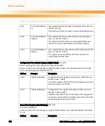
0x53
TstPatGenCtrlReg
Test Pattern Generator Control Register (8bit ) [Hw: asyn ,
WAck3, RAck3]
This registers controls test pattern transmission
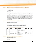
TSIP Interface Test Pattern Comparator Block (TstPatCmpBlk) [Hw: Cy0]
The TstPatCmp can be enabled to receive either static pattern or pseudo random pattern from a
remote generator. The Source can be a DSP or the Ser2TSIP block. The TSIP link is selectable between
0 and 59. The TSIP receive timeslot is selectable between 0 and 511. The TstPatCmpBlk includes a
PRBS pattern comparator (eleven stage LFSR with taps at the 9th and 11th stage). The pattern
comparator is able to synchronize itself to the receive bit stream. After synchronization 125
μ
s-
frames and errors are counted. A time of 125us delay has to be taken into account, till the
comparator has stopped after resetting TstPatCmpRxPatEn bit in TstPatCmpCtrlReg. Access via SPI-
bus from GlueFpga (occupies 256 Byte address area), hereof assigned to this block: 60...6F
Address
Acronym
Description
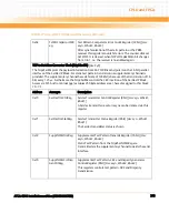
0x60
TstPatCmpLnkTsReg
Test Pattern Comparator Link and Timeslot Register (16bit)
[Hw: asyn , WAck3, RAck3]
This registers selects timeslot TSIP-link for the test pattern
reception.
0x62
TstPatRcvDatReg
Test Pattern Comparator Receive Data Register (8bit) [Hw:
asyn, WAck3, RAck3]
This registers holds the received pattern in the case of static
pattern reception. Not used in the case of pseudo random
pattern reception.
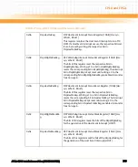
0x63
TstPatCmpDatReg
Test Pattern Comparator Data Register (8bit) [Hw: asyn,
WAck3, RAck3]
This registers holds the reference pattern in the case of static
pattern reception. Not used in the case of pseudo random
pattern reception.
0x64
TstPatCmpCtrlReg
Test Pattern Comparator Control Register (8bit) [Hw: asyn,
WAck3, RAck3]
This registers enables either static or pseudo random pattern
reception.
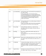
0x68
TstPatCmpSyncStaR
eg
Test Pattern Synchronization Status Register (32bit) [Hw: asyn
, WAck3, RAck3]
This registers indicates the synchronization status of the
received static pattern or the PRBS bit stream.
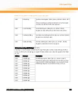
Table 8-174 Logic DSP FPGA Register Overview (continued)
Summary of Contents for ATCA-8310
Page 12: ...ATCA 8310 Installation and Use 6806800M72D Contents 12 Contents Contents ...
Page 26: ...ATCA 8310 Installation and Use 6806800M72D 26 List of Figures ...
Page 34: ...ATCA 8310 Installation and Use 6806800M72D About this Manual 34 About this Manual ...
Page 54: ...Hardware Preparation and Installation ATCA 8310 Installation and Use 6806800M72D 54 ...
Page 70: ...Controls Indicators and Connectors ATCA 8310 Installation and Use 6806800M72D 70 ...
Page 162: ...BIOS ATCA 8310 Installation and Use 6806800M72D 162 ...
Page 200: ...U Boot ATCA 8310 Installation and Use 6806800M72D 200 ...
Page 244: ...Intelligent Peripheral Management Controller ATCA 8310 Installation and Use 6806800M72D 244 ...
Page 438: ...CPLD and FPGA ATCA 8310 Installation and Use 6806800M72D 438 ...
Page 442: ...Replacing the Battery ATCA 8310 Installation and Use 6806800M72D 442 ...
Page 444: ...Related Documentation ATCA 8310 Installation and Use 6806800M72D 444 ...
Page 454: ...ATCA 8310 Installation and Use 6806800M72D Sicherheitshinweise 454 ...
Page 456: ...Index ATCA 8310 Installation and Use 6806800M72D 456 ...
Page 457: ...Index ATCA 8310 Installation and Use 6806800M72D 457 ...
Page 458: ...Index ATCA 8310 Installation and Use 6806800M72D 458 ...
Page 459: ......


