System Control
ARM DDI 0500D
Copyright © 2013-2014 ARM. All rights reserved.
4-132
ID021414
Non-Confidential
•
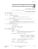
Only L1 Data data and L1 Data dirty RAMs can signal fatal errors, because all other RAM
instances are protected only by parity.
•
If two or more memory errors in the same RAM occur in the same cycle, only one error
is reported.
•
If two or more first memory error events from different RAMs occur in the same cycle,
one of the errors is selected arbitrarily.
•
If two or more memory error events from different RAMs, that do not match the RAMID,
Way, and index information in this register while the sticky Valid bit is set, occur in the
same cycle, then the Other error count field is incremented only by one.
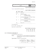
To access the CPUMERRSR_EL1:
MRS <Xt>, S3_1_c15_c2_2 ; Read CPUMERRSR into Xt
MSR S3_1_c15_c2_2, <Xt> ; Write Xt to CPUMERRSR
4.3.81
L2 Memory Error Syndrome Register
The L2MERRSR_EL1 characteristics are:
Purpose
Holds information about ECC errors on the:
•
L2 data RAMs.
•
L2 tag RAMs.
•
SCU snoop filter RAMs.
Usage constraints
This register is accessible as follows:
Configurations
The L2MERRSR_EL1 is:
•
Mapped to the AArch32 L2MERRSR register. See
L2 Memory
Error Syndrome Register
on page 4-276
.
•
There is one copy of this register that is used in both Secure and
Non-secure states.
•
A write of any value to the register updates the register to
0x10000000
.
Attributes
L2MERRSR_EL1 is a 64-bit register.
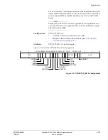
Figure 4-74
shows the L2MERRSR_EL1 bit assignments.
Figure 4-74 L2MERRSR_EL1 bit assignments
EL0
EL1
(NS)
EL1
(S)
EL2
EL3
(SCR.NS = 1)
EL3
(SCR.NS = 0)
-
RW
RW
RW
RW
RW
Fatal
24 23 22 21
Other error
count
Repeat error
count
31
32
0
63
RES
0
47
48
40 39
30
Valid
RAMID
18 17
CPUID/Way
RAM address
2
3
62
RES
0
RES
0
16
RES
0


