SPORT Control Registers and Data Buffers
9-44
ADSP-2126x SHARC Processor Hardware Reference
4. Wait one cycle. A
NOP
instruction can be used to cause this delay; if
a
NOP
is not inserted, the processor core is paused for one cycle any-
way. This allows the serial port companding hardware to reload the
transmit buffer with the companded value.
5. Read the 8-bit companded value from the transmit buffer.
To expand data in place, use the same sequence of operations (above) with
the receive buffer instead of the transmit buffer. When expanding data in
this way, set the appropriate serial word length (
SLEN
) in the
SPCTLx
Con-
trol register.
With companding enabled, interfacing the serial port to a codec requires
little additional programming effort. If companding is not selected, two
formats are available for received data words of fewer than 32 bits—one
that fills unused MSBs with zeros, and another that sign-extends the MSB
into the unused bits.
SPORT Control Registers and Data Buffers
The ADSP-2126x has six serial ports. Each SPORT has two data paths
corresponding to channel A and channel B. These data buffers are
TXSPxA
and
RXSPxA
(primary) and
TXSPxB
and
RXSPxB
(secondary). Channel A and
B in all six SPORTS operate synchronously to their respective
SPORTx_CLK
and
FSx
signals. Companding is supported only on primary A channels.
The registers used to control and configure the serial ports are part of the
IOP register set. Each SPORT has its own set of 32-bit control registers
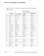
and data buffers. The SPORT registers are described in
The SPORT control registers are programmed by writing to the appropri-
ate address in memory. The symbolic names of the registers and individual
control bits can be used in programs. The definitions for these symbols are
contained in the file
def2126x.h
located in the
INCLUDE
directory of the
Summary of Contents for ADSP-21261 SHARC
Page 30: ...Contents xxx ADSP 2126x SHARC Processor Hardware Reference ...
Page 40: ...Register Diagram Conventions xl ADSP 2126x SHARC Processor Hardware Reference ...
Page 58: ...Differences From Previous SHARCs 1 18 ADSP 2126x SHARC Processor Hardware Reference ...
Page 112: ...Secondary Processing Element PEy 2 54 ADSP 2126x SHARC Processor Hardware Reference ...
Page 178: ...Summary 3 66 ADSP 2126x SHARC Processor Hardware Reference ...
Page 204: ...DAG Instruction Summary 4 26 ADSP 2126x SHARC Processor Hardware Reference ...
Page 322: ...Setting Up DMA 7 32 ADSP 2126x SHARC Processor Hardware Reference ...
Page 436: ...SPORT Programming Examples 9 86 ADSP 2126x SHARC Processor Hardware Reference ...
Page 521: ...ADSP 2126x SHARC Processor Hardware Reference 11 31 Input Data Port rts IDP_ISR end ...
Page 522: ...Input Data Port Programming Example 11 32 ADSP 2126x SHARC Processor Hardware Reference ...
Page 590: ...Timer Programming Examples 14 20 ADSP 2126x SHARC Processor Hardware Reference ...
Page 796: ...I O Processor Registers A 174 ADSP 2126x SHARC Processor Hardware Reference ...
Page 800: ...B 4 ADSP 2126x SHARC Processor Core Manual ...
Page 846: ...Index I 36 ADSP 2126x SHARC Processor Hardware Reference ...


