UM353-1B
Function Blocks
April 2012
3-77
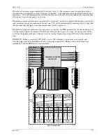
When the last sequencer step is completed, SC will be set high (1). The sequencer cannot be moved past the last
step unless the reset input R goes high (1) forcing it to position 1. The sequencer can be moved forward only when
in position 1. Network communications will allow the sequencer to be moved to a new step and the remaining time
of the current step to be changed to a new value.
When discrete groups are used and a step is desired as ‘timed only’, one discrete input should be used to prevent the
input mask from moving the sequencer to the next step. This can be accomplished by requiring a high (1) input and
then not connecting that input, since unconnected inputs will be treated as 0.
When discrete groups are used and a step is desired as ‘event only’, the TIMe parameter for the step should be set to
0.0. The Analog Output will remain at the AEP value of the previous step or, if at step 1, the Analog value will be
0.0. When the sequencer advances to the next step, the Analog Output will go to the AEP value for the completed
step.
POWER UP - During a warm start, if PU LAST is set to YES, all outputs, step number, track variable, and
remaining step time will be initialized at the last values prior to power fail. During a cold start all outputs are
initialized to 0 and the PRSEQ is in a reset condition.
TV
TC
SF
SB
GS
SN
T
rack
V
ariable
T
rack
C
ommand
S
tep
F
orward
S
tep
B
ackward
S
tep
N
umber
S
tep
N
umber
A
nalog
Ou
tput
S
tep
P
ulse
AO
SN
SP
PROGRAM & SEQUENCE
CONTROLLER
00
01
02
03
04
05
06
07
08
09
0A
0B
0C
0D
0E
0F
10
FF
00
01
02
03
04
05
06
07
08
09
0A
0B
0C
0D
0E
0F
10
FF
Discrete Inputs
Discrete Outputs
Step 006
AEP
= 300.00
TIM
e = 2.45
Input
Mask
Output
Mask
Group 1
2E5B
003E
01 = 0
02 = 1
00 = 1
..
01 = 1
02 = 1
00 = 1
..
Step 007
AEP
= 325.00
TIM
e = 5.25
Input
Mask
Output
Mask
Group 1
0034
00E8
01 = 0
02 = 1
00 = 0
..
01 = 0
02 = 1
00 = 0
..
Step 008
AEP
= 325.00
TIM
e = 0.0
Input
Mask
Output
Mask
Group 1
13D2
003E
01 = 1
02 = 0
00 = 0
..
01 = 1
02 = 1
00 = 1
..
Step 009
AEP
= 340.00
TIM
e = 25.0
Input
Mask
Output
Mask
Group 1
327A
003E
01 = 0
02 = 1
00 = 1
..
01 = 1
02 = 1
00 = 1
..
Group 2
Group 2
Group 2
Group 2
..
..
..
..
BLOCK DIAGRAM
Gr
o
u
p 1
G
ro
up 1
S
tep
T
ime
RT
R
emaining
T
ime
ST
A
nalog
O
utput
AO
H
R
R
eset
H
old
G
o to
S
tep
.
.
Analog
Output
RN
LR
R
ecipe
N
umber
L
oad
R
ecipe
Rev. 2
Содержание 353
Страница 12: ...Contents UM353 1B x April 2012 ...
Страница 22: ...Introduction UM353 1B April 2012 1 10 ...
Страница 30: ...Configuration Overview UM353 1B April 2012 2 8 ...
Страница 122: ...Function Blocks UM353 1B April 2012 3 92 ...
Страница 168: ...Data Mapping UM353 1B April 2012 6 28 ...
Страница 204: ...Controller and System Test UM353 1B April 2012 9 8 ...
Страница 222: ...Calibration UM353 1B April 2012 11 4 ...
Страница 226: ...Circuit Description UM353 1B April 2012 12 4 ...
Страница 238: ...Model Designation and Specifications UM353 1B April 2012 13 12 EC Declaration of Conformity ...
Страница 239: ...UM353 1B Model Designation and Specifications April 2012 13 13 Annex A to the EC Declaration of Conformity ...
Страница 240: ...Model Designation and Specifications UM353 1B April 2012 13 14 ...
Страница 244: ...Abbreviations And Acronyms UM353 1B 14 4 April 2012 ...

