


Function Blocks
UM353-1B
April
2012
3-68
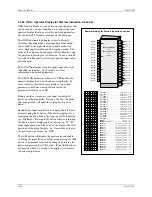
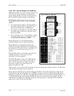
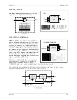
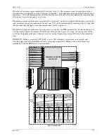
3.2.66 PCOM - Phase COMmunication
The Phase Communication
PCOM
function block is
available on a one per loop basis to enable
communication with a higher level device, such as a PC
running a batch management software program. When
the controller configuration is structured such that logic
operations are partitioned in small phase operations, the
PCOM block facilitates the interface between the logic
controlling the overall phase operations for the batch
and the logic performing the control logic for each
phase.
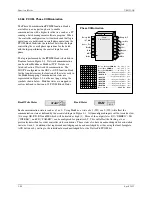
The logic performed by the
PCOM
block is detailed in
Boolean form in Figure 3-1. Network communication
can be either Modbus or Modbus/TCP. Details are
listed in Section 5 Network Communications. The
LOOP # configured in the ODC or ODS function block
for the loop determines the location of the status coils in
the Modbus mapping. Communication states are
represented in Figure 3-1, on the next page, using the
symbols shown below. Modbus states are mapped in
coils as defined in Section 6.3.9 PCOM Block Status.
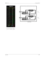
Read/Write States
R 0
W 1
W 0
START
Read States
R 1/0
RUN
Each communication state is read as a 1 or 0. Using Modbus, a write of a 1 (W1) or a 0 (W0) will affect the
communication state as defined by the associated logic in Figure 3-1. All unconfigured inputs will be treated as low
(0) except OK, RD, RN and HE which will be treated as high (1). Three of the output states, EO (“EMERG”), IK
(“INTRLK”), and FD (“FAILED”) can be configured for priorities 0-5. This will affect the flashing, etc. as
previously described for other controller status conditions. These states also have unacknowledged bits as detailed
in status word 2. Conditions that require acknowledging can be acknowledged by either using the local faceplate
ACK button or by writing to the individual not acknowledged bit or the Not Ack’d PCOM bit.
E
merg.
O
R
Phase COMunication
EO
Phase
Communication
PCOM
EO
INT_
OK
OK
P
I O
R
O
E
E
merg.
O
verride
PRIOR
ity ... 0,1,2,3,4,5 (4)
P
hase_
F
ail
PF
IK
I
nterloc
K
ed
FD
F
aile
D
R
T
U
P
N
I
INPUT EO
............
loop tag.block tag.output
(
null
)
E O
R
ea
D
y
RD
R
u
N
RN
HE
ld
HE
D
o
N
e
DN
RS
R
e
S
et
EN
EN
abled
ST
ST
art
HO
HO
ld
P
T
U
P
N
I
O
T
U
P
N
I
K
F
T
U
P
N
I
T
U
P
N
I
R D
R N
D
T
U
P
N
I
H
T
U
P
N
I
E
N
INPUT PF
............
loop tag.block tag.output
(
null
)
INPUT OK
............
loop tag.block tag.output
(
null
)
INPUT RN
............
loop tag.block tag.output
(
null
)
INPUT RD
............
loop tag.block tag.output
(
null
)
INPUT DN
............
loop tag.block tag.output
(
null
)
INPUT HE
............
loop tag.block tag.output
(
null
)
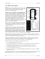
S
E
N
E
xec.
S
eq.
N
o. .................... 000 to 250 (000)
E
merg.
O
R
I
nterloc
K
ed
PRIOR
ity ........... 0,1,2,3,4,5 (4)
D
evice
F
ail
PRIOR
ity ............ 0,1,2,3,4,5 (4)
P
I O
R
R
P
I O
R
R
I K
D F
Содержание 353
Страница 12: ...Contents UM353 1B x April 2012 ...
Страница 22: ...Introduction UM353 1B April 2012 1 10 ...
Страница 30: ...Configuration Overview UM353 1B April 2012 2 8 ...
Страница 122: ...Function Blocks UM353 1B April 2012 3 92 ...
Страница 168: ...Data Mapping UM353 1B April 2012 6 28 ...
Страница 204: ...Controller and System Test UM353 1B April 2012 9 8 ...
Страница 222: ...Calibration UM353 1B April 2012 11 4 ...
Страница 226: ...Circuit Description UM353 1B April 2012 12 4 ...
Страница 238: ...Model Designation and Specifications UM353 1B April 2012 13 12 EC Declaration of Conformity ...
Страница 239: ...UM353 1B Model Designation and Specifications April 2012 13 13 Annex A to the EC Declaration of Conformity ...
Страница 240: ...Model Designation and Specifications UM353 1B April 2012 13 14 ...
Страница 244: ...Abbreviations And Acronyms UM353 1B 14 4 April 2012 ...