


M0A21/M0A23 Series
May 06, 2022
Page
624
of 746
Rev 1.02
M0
A21
/M
0
A
2
3
SE
RIES
TEC
H
NICAL
RE
FEREN
C
E
M
ANUAL
tolerance df is the defined by two conditions (both shall be met):
𝐼: 𝑑𝑓 <=
min (Phase_Seg1, Phase_Seg2)
2 ∗ (13 ∗ bit_time − 𝑃ℎ𝑎𝑠𝑒_𝑆𝑒𝑔2
𝐼𝐼: 𝑑𝑓 <=
SJW
20 ∗ bit_tim
Note:
These conditions base on the APB cock =
f
osc.
It has to be considered that SJW may not be larger than the smaller of the Phase Buffer Segments and
that the Propagation Time Segment limits that part of the bit time that may be used for the Phase Buffer
Segments.
The combination Prop_Seg = 1 and Phase_Seg1 = Phase_Seg2 = SJW = 4 allows the largest possible
oscillator tolerance of 1.58%. This combination with a Propagation Time Segment of only 10% of the bit
time is not suitable for short bit times; it can be used for bit rates of up to 125 Kbit/s (bit time = 8us) with
a bus length of 40 m.
Configuring the CAN Protocol Controller
In most CAN implementations and also in the C_CAN, the bit timing configuration is programmed in two
register bytes. The sum of Prop_Seg and Phase_Seg1 (as TSEG1 (CAN_BTIME[11:8])) is combined
with Phase_Seg2 (as TSEG2 (CAN_BTIME[14:12])) in one byte, SJW (CAN_BTIME[7:6]) and BRP
(CAN_BTIME[5:0]) are combined in the other byte.
In these bit timing registers, the four components TSEG1, TSEG2, SJW and BRP have to be
programmed to a numerical value that is one less than its functional value. Therefore, instead of values
in the range of [1..n], values in the range of [0..n-1] are programmed. That way, e.g. SJW (functional
range of [1..4]) is represented by only two bits.
Therefore the length of the bit time is (programmed values) [TSEG1 + TSEG2 + 3] tq or (functional
values) [Sy Pr Phas Phase_Seg2] tq.
Baudrate_Prescaler
APB Clock
Configuration (BRP)
Bit
Timing
Logic
Received_Data
Transmit_Data
Sample_Point
Sample_Bit
Sync_Mode
Bit_to_send
Bus_Off
Bit
Stream
Processor
Control
Status
Shift-Register
Received_Data_Bit
Send_Message
Control
Next_Data_Bit
Received_Message
Configuration (TSEG1, TSEG2,SJW)
Scaled_Clock (
t
q
)
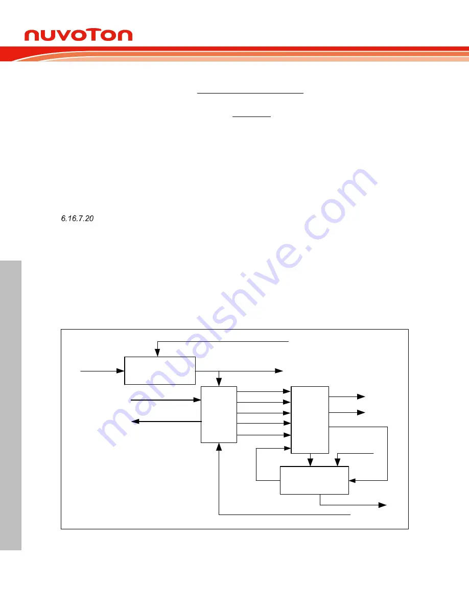
Figure 6.16-11
Structure of the CAN Core’s CAN Protocol Controller
The data in the bit timing registers is the configuration input of the CAN protocol controller. The Baud
Rate Prescaler (configured by BRP) defines the length of the time quantum, the basic time unit of the


