


M0A21/M0A23 Series
May 06, 2022
Page
540
of 746
Rev 1.02
M0
A21
/M
0
A
2
3
SE
RIES
TEC
H
NICAL
RE
FEREN
C
E
M
ANUAL
is equal to or greater than the value of SLVTOCNT (USPI_PROTCTL[25:16]) before one
word transaction is done, the Slave time-out interrupt event occurs and the SLVTOIF
(USPI_PROTSTS[5]) will be set to 1.
Buffer-Related Interrupts
The buffer-related interrupts are available if there is transmit/receive buffer in USCI controller.
Receive buffer overrun interrupt
If there is receive buffer overrun event, RXOVIF (USPI_BUFSTS[3]) will be set as 1. It can
be cleared by write 1 into it.
Transmit buffer under-run interrupt
If there is transmit buffer under-run event, TXUDRIF (USPI_BUFSTS[11]) will be set as 1.
It can be cleared by write 1 into it.
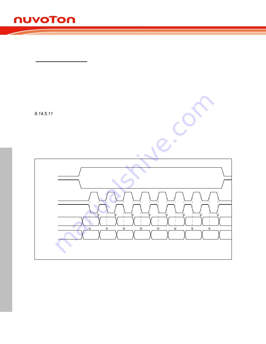
Timing Diagram
The slave select signal of USCI SPI protocol is active high by default, and it can be inverted by CTLOINV
(USPI_LINECTL[7]) setting.
The idle state of serial bus clock and the serial bus clock edge used for transmit/receive data can be
configured by setting SCLKMODE (USPI_PROTCTL[7:6]). The bit length of a transaction word data is
determined by DWIDTH (USPI_LINECTL[11:8]), and data bit transfer sequence is determined by LSB
(USPI_LINECTL[0]). Four SPI timing diagrams for Master/Slave operations and the related settings are
shown below.
SPI_CLK
SPI_MISO
SPI_MOSI
TX[6]
TX[4]
TX[3]
TX[2]
LSB
TX[0]
RX[6]
RX[4]
RX[2]
LSB
RX[0]
MSB
RX[7]
RX[3]
MSB
TX[7]
SPI_SS
SCLKMODE=0x0
TX[5]
RX[5]
TX[1]
RX[1]
Master Mode: FUNMODE=0x1, SLAVE=0,
LSB=0, DWIDTH=0x8
SCLKMODE=0x2
CTLOINV=0
CTLOINV=1
Figure 6.14-16 SPI Timing in Master Mode


