Lake Shore Model 321 Autotuning Temperature Controller User’s Manual
D-16
Application Notes
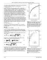
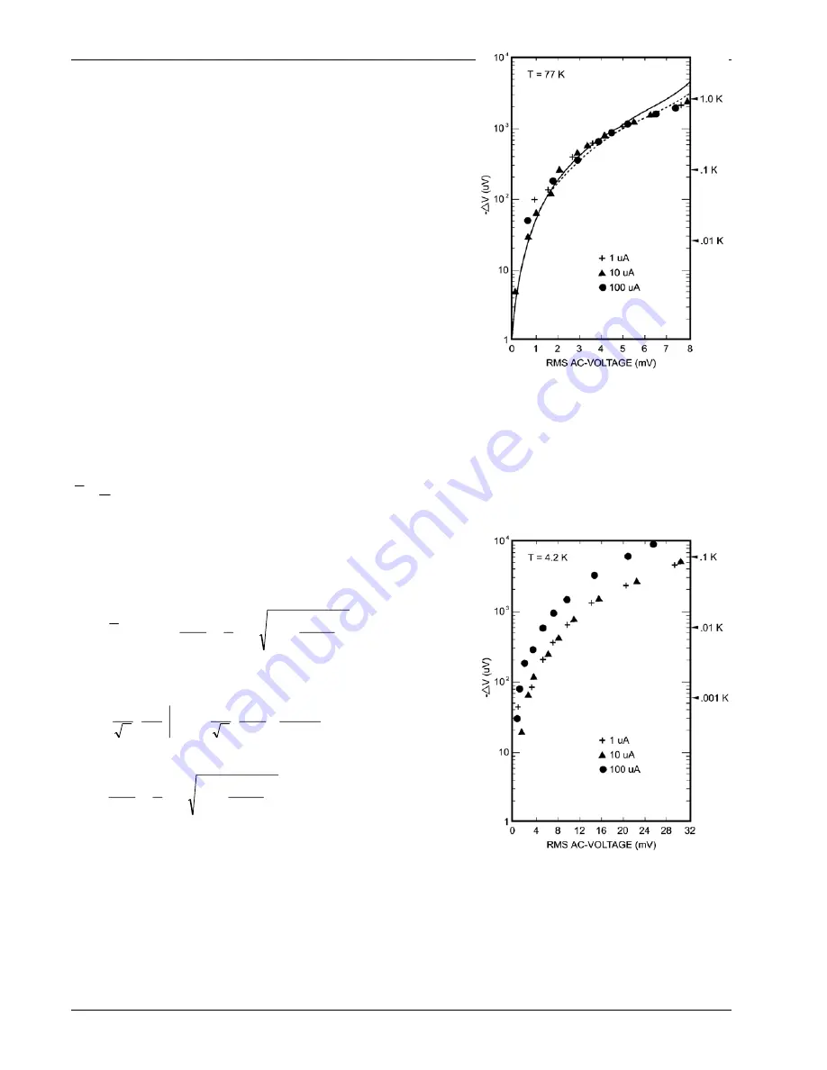
The measured offset voltages shown in Figs. 4 and 6 can be understood
by using the well-known result from
p-n
junction theory:
I = I
s
[exp(eV / nkT) - 1]
(1)
where
I
= the forward current through the junction,
I
s
= the reverse
saturation current,
e
= the electron charge,
V
= the voltage across the
junction,
k
= Boltzmann's constant, and
T
= the absolute temperature.
n
is a parameter depending on the location of the generation and
recombination of the electrons and holes and typically has a value
between 1 and 2. This expression for the IV characteristics of a
p-n
junction is valid from approximately 40 K to above 300 K for the silicon
diodes discussed here. Below 40 K, a new conduction mechanism
becomes dominant, suggesting the influence of impurity conduction,
carrier freezeout, increased ohmic behavior of the bulk material, and
p-i-
n
diode type behavior.
1-6
The only adjustable parameter in Eq. 1 which is necessary for the
present analysis is the parameter
n
. This parameter can be determined
quite easily from the IV characteristics of the silicon diode temperature
sensor. The parameter
I
s
is eliminated by normalizing the IV curve to an
arbitrarily chosen point on the curve. The value of n = 1.8 was found to
give a relatively good fit to the IV data for both 305 and 77 K and has
been assumed in the present discussion.7 Equation (1) can now be
solved for V(I):
V(I) = (nkT / e)ln(I / I
s
+ 1)
(2)
Substituting a dc current with an ac modulation, I
dc
+ I
ac
cos
ω
t
, the
average voltage read by the voltmeter in the dc voltage mode can be
calculated from:
V
T
V I
I
t dt
dc
ac
T
=
+
z
1
0
(
cos
)
ω
(3)
where T = the period of integration of the voltmeter or approximately
2
π
/
ω
. Implied in this derivation is the assumption that
ω
is sufficiently
small so that effects from diode capacitance (on the order of picofarads)
can be ignored.
On carrying out the integration of Eq. (3) and subtracting V(I
dc
), the dc
offset voltage is:
∆
V V V I
nkT
e
eV
nkT
dc
rms
= −
=
+
−
F
HG
I
KJ
F
H
GG
I
K
JJ
L
N
MM
O
Q
PP
(
)
ln
1
2
1
1 2
2
(4)
where I
ac
≤
I
dc
+ I
s
. If a small signal (linear) model is used, the rms
voltage across the diode can be easily related to I
ac
:
V
I
dV
dI
nkT
e
I
I
I
rms
ac
ac
dc
s
I Idc
=
F
HG
I
KJ
=
F
HG
I
KJ
+
F
HG
I
KJ
=
2
1
2
(5)
Evaluation of Eq. (5) and substitution back into (4) yields:
∆
V
nkT
e
eV
nkT
rms
=
+
−
F
HG
I
KJ
F
H
GG
I
K
JJ
L
N
MM
O
Q
PP
ln
1
2
1
1 2
2
(6)
where 2(eV
rms
/ nkT)
2
≤
1 for a physical solution. Equation (6) predicts an
offset voltage which is independent of both frequency and dc operating
current and is shown plotted in Fig. 4 by the solid line. The agreement
with the experimental measurements is quite good, verifying the overall
picture as to the effect of induced currents on diode temperature
sensors. The results recorded at 305 K are described equally well by
Eq. (6).
FIGURE 4.
DC offset voltage as a function of rms ac
voltage across a silicon diode temperature sensor
operating at 77 K. The symbols represent data
recorded at three different dc operating currents with
a 60 Hz signal superimposed. The solid curve gives
small signal model results while the dashed curve
represents the extended calculations. Equivalent
temperature errors are indicated along the right
edge.
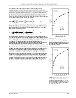
FIGURE 5.
DC offset voltage as a function of rms ac
voltage across a silicon diode temperature sensor
operating at 4.2 K. The symbols represent data
recorded at three different dc operating currents with
a 60 Hz signal superimposed. Equivalent
temperature errors are indicated along the right
edge.

