


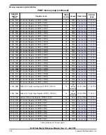


Table 10-1. Reference links to related information (continued)
Topic
Related module
Reference
Clocking
Register access
Peripheral bus
controller
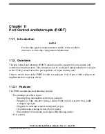
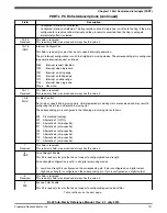
10.2.1 Port control and interrupt module features
• 32-pin ports
NOTE
Not all pins are available on the device. See the following
section for details.
• Each port is assigned one interrupt.
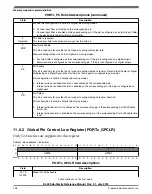
The reset state and read/write characteristics of the fields within the PORTx_PCRn
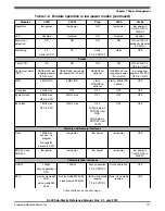
registers is summarized in the table below.
Table 10-2. Port control register configuration summary
This field
of
PORTx_PC
Rn
Generally
resets to
Except for
Resets to
Configurability
PS
1
PTA0
0
Fixed—All are read only.
PE
0
PTA0 and PTA2
1
Yes—All GPIOs are
configurable
DSE
0
No exceptions—all DSE are cleared on reset.
—
4 pins are configurable for
High Drive (PTB0, PTB1,
PTA12 and PTA13). All
others are fixed for Normal
Drive and the associated
DSE bit is read only.
SRE
1
PTA2, PTA5, PTA6, PTA7, PTB0
0
No— All GPIOs are not
configurable
MUX
000
PTA0, PTA2, and PTB5
011
Yes— All GPIOs are
configurable. MSB (bit2) of
MUX is not writable and
always reads 0.
PFE
0
No exceptions—all PFE are cleared on reset.
—
The GPIO shared with
NMI_b pin is configurable.
All other GPIOs are fixed
and read only.
IRQC
000
No exceptions—all are cleared on reset.
—
Yes
ISF
0
No exceptions—all are cleared on reset.
—
—
Signal multiplexing integration
KL02 Sub-Family Reference Manual, Rev. 2.1, July 2013
124
Freescale Semiconductor, Inc.
Содержание KKL02Z32CAF4R
Страница 2: ...KL02 Sub Family Reference Manual Rev 2 1 July 2013 2 Freescale Semiconductor Inc...
Страница 24: ...KL02 Sub Family Reference Manual Rev 2 1 July 2013 24 Freescale Semiconductor Inc...
Страница 36: ...Orderable part numbers KL02 Sub Family Reference Manual Rev 2 1 July 2013 36 Freescale Semiconductor Inc...
Страница 76: ...Human machine interfaces HMI KL02 Sub Family Reference Manual Rev 2 1 July 2013 76 Freescale Semiconductor Inc...
Страница 94: ...Module clocks KL02 Sub Family Reference Manual Rev 2 1 July 2013 94 Freescale Semiconductor Inc...
Страница 142: ...Functional description KL02 Sub Family Reference Manual Rev 2 1 July 2013 142 Freescale Semiconductor Inc...
Страница 188: ...Memory map and register descriptions KL02 Sub Family Reference Manual Rev 2 1 July 2013 188 Freescale Semiconductor Inc...
Страница 214: ...Application information KL02 Sub Family Reference Manual Rev 2 1 July 2013 214 Freescale Semiconductor Inc...
Страница 222: ...Memory map register descriptions KL02 Sub Family Reference Manual Rev 2 1 July 2013 222 Freescale Semiconductor Inc...
Страница 256: ...Memory map and register definition KL02 Sub Family Reference Manual Rev 2 1 July 2013 256 Freescale Semiconductor Inc...
Страница 300: ...Functional description KL02 Sub Family Reference Manual Rev 2 1 July 2013 300 Freescale Semiconductor Inc...
Страница 532: ...Functional description KL02 Sub Family Reference Manual Rev 2 1 July 2013 532 Freescale Semiconductor Inc...
Страница 534: ...KL02 Sub Family Reference Manual Rev 2 1 July 2013 534 Freescale Semiconductor Inc...


