


The configuration of each pin control register is retained when the PORT module is
disabled.
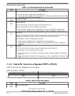
11.6.2 Global pin control
The two global pin control registers allow a single register write to update the lower half
of the pin control register on up to sixteen pins, all with the same value.
The global pin control registers are designed to enable software to quickly configure
multiple pins within the one port for the same peripheral function. However, the interrupt
functions cannot be configured using the global pin control registers.
The global pin control registers are write-only registers, that always read as zero.
11.6.3 External interrupts
The external interrupt capability of the PORT module is available in all digital pin
muxing modes provided the PORT module is enabled.
Each pin can be individually configured for any of the following external interrupt
modes:
• Interrupt disabled, default out of reset
• Active high level sensitive interrupt
• Active low level sensitive interrupt
• Rising edge sensitive interrupt
• Falling edge sensitive interrupt
• Rising and falling edge sensitive interrupt
The interrupt status flag is set when the configured edge or level is detected on the pin .
When not in Stop mode, the input is first synchronized to the bus clock to detect the
configured level or edge transition.
The PORT module generates a single interrupt that asserts when the interrupt status flag
is set for any enabled interrupt for that port. The interrupt negates after the interrupt status
flags for all enabled interrupts have been cleared by writing a logic 1 to the ISF flag in
either the PORT_ISFR or PORT_PCRn registers.
During Stop mode, the interrupt status flag for any enabled interrupt is asynchronously
set if the required level or edge is detected. This also generates an asynchronous wakeup
signal to exit the Low-Power mode.
Chapter 11 Port Control and Interrupts (PORT)
KL02 Sub-Family Reference Manual, Rev. 2.1, July 2013
Freescale Semiconductor, Inc.
141
Содержание KKL02Z32CAF4R
Страница 2: ...KL02 Sub Family Reference Manual Rev 2 1 July 2013 2 Freescale Semiconductor Inc...
Страница 24: ...KL02 Sub Family Reference Manual Rev 2 1 July 2013 24 Freescale Semiconductor Inc...
Страница 36: ...Orderable part numbers KL02 Sub Family Reference Manual Rev 2 1 July 2013 36 Freescale Semiconductor Inc...
Страница 76: ...Human machine interfaces HMI KL02 Sub Family Reference Manual Rev 2 1 July 2013 76 Freescale Semiconductor Inc...
Страница 94: ...Module clocks KL02 Sub Family Reference Manual Rev 2 1 July 2013 94 Freescale Semiconductor Inc...
Страница 142: ...Functional description KL02 Sub Family Reference Manual Rev 2 1 July 2013 142 Freescale Semiconductor Inc...
Страница 188: ...Memory map and register descriptions KL02 Sub Family Reference Manual Rev 2 1 July 2013 188 Freescale Semiconductor Inc...
Страница 214: ...Application information KL02 Sub Family Reference Manual Rev 2 1 July 2013 214 Freescale Semiconductor Inc...
Страница 222: ...Memory map register descriptions KL02 Sub Family Reference Manual Rev 2 1 July 2013 222 Freescale Semiconductor Inc...
Страница 256: ...Memory map and register definition KL02 Sub Family Reference Manual Rev 2 1 July 2013 256 Freescale Semiconductor Inc...
Страница 300: ...Functional description KL02 Sub Family Reference Manual Rev 2 1 July 2013 300 Freescale Semiconductor Inc...
Страница 532: ...Functional description KL02 Sub Family Reference Manual Rev 2 1 July 2013 532 Freescale Semiconductor Inc...
Страница 534: ...KL02 Sub Family Reference Manual Rev 2 1 July 2013 534 Freescale Semiconductor Inc...


