


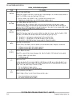


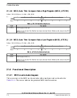


21.3.5 MCG Control 6 Register (MCG_C6)
Address: 4006_4000h base + 5h offset = 4006_4005h
Bit
7
6
5
4
3
2
1
0
Read
Write
Reset
0
0
0
0
0
0
0
0
MCG_C6 field descriptions
Field
Description
7–6
Reserved
Reserved
This field is reserved.
This read-only field is reserved and always has the value 0.
5
CME
Clock Monitor Enable
Determines if a reset request is made following a loss of external clock indication. The CME bit should
only be set to a logic 1 when the MCG is in an operational mode that uses the external clock (FEE, FBE,
or BLPE). Whenever the CME bit is set to a logic 1, the value of the RANGE bits in the C2 register should
not be changed. CME bit should be set to a logic 0 before the MCG enters any Stop mode. Otherwise, a
reset request may occur when in Stop mode. CME should also be set to a logic 0 before entering VLPR or
VLPW power modes if the MCG is in BLPE mode.
0
External clock monitor is disabled.
1
Generate a reset request on loss of external clock.
Reserved
Reserved
This field is reserved.
This read-only field is reserved and always has the value 0.
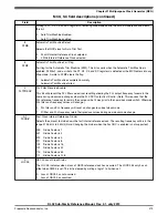
21.3.6 MCG Status Register (MCG_S)
Address: 4006_4000h base + 6h offset = 4006_4006h
Bit
7
6
5
4
3
2
1
0
Read
Write
Reset
0
0
0
1
0
0
0
0
MCG_S field descriptions
Field
Description
7–5
Reserved
Reserved
This field is reserved.
This read-only field is reserved and always has the value 0.
Table continues on the next page...
Chapter 21 Multipurpose Clock Generator (MCG)
KL02 Sub-Family Reference Manual, Rev. 2.1, July 2013
Freescale Semiconductor, Inc.
271
Содержание KKL02Z32CAF4R
Страница 2: ...KL02 Sub Family Reference Manual Rev 2 1 July 2013 2 Freescale Semiconductor Inc...
Страница 24: ...KL02 Sub Family Reference Manual Rev 2 1 July 2013 24 Freescale Semiconductor Inc...
Страница 36: ...Orderable part numbers KL02 Sub Family Reference Manual Rev 2 1 July 2013 36 Freescale Semiconductor Inc...
Страница 76: ...Human machine interfaces HMI KL02 Sub Family Reference Manual Rev 2 1 July 2013 76 Freescale Semiconductor Inc...
Страница 94: ...Module clocks KL02 Sub Family Reference Manual Rev 2 1 July 2013 94 Freescale Semiconductor Inc...
Страница 142: ...Functional description KL02 Sub Family Reference Manual Rev 2 1 July 2013 142 Freescale Semiconductor Inc...
Страница 188: ...Memory map and register descriptions KL02 Sub Family Reference Manual Rev 2 1 July 2013 188 Freescale Semiconductor Inc...
Страница 214: ...Application information KL02 Sub Family Reference Manual Rev 2 1 July 2013 214 Freescale Semiconductor Inc...
Страница 222: ...Memory map register descriptions KL02 Sub Family Reference Manual Rev 2 1 July 2013 222 Freescale Semiconductor Inc...
Страница 256: ...Memory map and register definition KL02 Sub Family Reference Manual Rev 2 1 July 2013 256 Freescale Semiconductor Inc...
Страница 300: ...Functional description KL02 Sub Family Reference Manual Rev 2 1 July 2013 300 Freescale Semiconductor Inc...
Страница 532: ...Functional description KL02 Sub Family Reference Manual Rev 2 1 July 2013 532 Freescale Semiconductor Inc...
Страница 534: ...KL02 Sub Family Reference Manual Rev 2 1 July 2013 534 Freescale Semiconductor Inc...


