


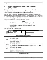


• The Low Voltage Detect Flag in the Low Voltage Status and Control 1 Register
(LVDSC1[LVDF]) operates in a level sensitive manner. LVDSC1[LVDF] is set
when the supply voltage falls below the selected trip point (VLVD).
LVDSC1[LVDF] is cleared by writing 1 to LVDSC1[LVDACK], but only if the
internal supply has returned above the trip point; otherwise, LVDSC1[LVDF]
remains set.
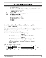
• The Low Voltage Warning Flag (LVWF) in the Low Voltage Status and Control 2
Register (LVDSC2[LVWF]) operates in a level sensitive manner. LVDSC2[LVWF]
is set when the supply voltage falls below the selected monitor trip point (VLVW).
LVDSC2[LVWF] is cleared by writing one to LVDSC2[LVWACK], but only if the
internal supply has returned above the trip point; otherwise, LVDSC2[LVWF]
remains set.
14.3.1 LVD reset operation
By setting LVDSC1[LVDRE], the LVD generates a reset upon detection of a low-voltage
condition. The low-voltage detection threshold is determined by LVDSC1[LVDV]. After
an LVD reset occurs, the LVD system holds the MCU in reset until the supply voltage
rises above this threshold. The LVD field in the SRS register of the RCM module
(RCM_SRS0[LVD]) is set following an LVD or power-on reset.
14.3.2 LVD interrupt operation
By configuring the LVD circuit for interrupt operation (LVDIE set and LVDRE clear),
LVDSC1[LVDF] is set and an LVD interrupt request occurs upon detection of a low
voltage condition. The LVDF bit is cleared by writing one to the LVDSC1[LVDACK]
bit.
14.3.3 Low-voltage warning (LVW) interrupt operation
The LVD system contains a Low-Voltage Warning Flag (LVWF) in the Low Voltage
Detect Status and Control 2 Register to indicate that the supply voltage is approaching,
but is above, the LVD voltage. The LVW also has an interrupt, which is enabled by
setting LVDSC2[LVWIE]. If enabled, an LVW interrupt request occurs when
LVDSC2[LVWF] is set. LVDSC2[LVWF] is cleared by writing 1 to
LVDSC2[LVWACK].
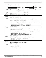
LVDSC2[LVWV] selects one of the four trip voltages:
Low-voltage detect (LVD) system
KL02 Sub-Family Reference Manual, Rev. 2.1, July 2013
182
Freescale Semiconductor, Inc.
Содержание KKL02Z32CAF4R
Страница 2: ...KL02 Sub Family Reference Manual Rev 2 1 July 2013 2 Freescale Semiconductor Inc...
Страница 24: ...KL02 Sub Family Reference Manual Rev 2 1 July 2013 24 Freescale Semiconductor Inc...
Страница 36: ...Orderable part numbers KL02 Sub Family Reference Manual Rev 2 1 July 2013 36 Freescale Semiconductor Inc...
Страница 76: ...Human machine interfaces HMI KL02 Sub Family Reference Manual Rev 2 1 July 2013 76 Freescale Semiconductor Inc...
Страница 94: ...Module clocks KL02 Sub Family Reference Manual Rev 2 1 July 2013 94 Freescale Semiconductor Inc...
Страница 142: ...Functional description KL02 Sub Family Reference Manual Rev 2 1 July 2013 142 Freescale Semiconductor Inc...
Страница 188: ...Memory map and register descriptions KL02 Sub Family Reference Manual Rev 2 1 July 2013 188 Freescale Semiconductor Inc...
Страница 214: ...Application information KL02 Sub Family Reference Manual Rev 2 1 July 2013 214 Freescale Semiconductor Inc...
Страница 222: ...Memory map register descriptions KL02 Sub Family Reference Manual Rev 2 1 July 2013 222 Freescale Semiconductor Inc...
Страница 256: ...Memory map and register definition KL02 Sub Family Reference Manual Rev 2 1 July 2013 256 Freescale Semiconductor Inc...
Страница 300: ...Functional description KL02 Sub Family Reference Manual Rev 2 1 July 2013 300 Freescale Semiconductor Inc...
Страница 532: ...Functional description KL02 Sub Family Reference Manual Rev 2 1 July 2013 532 Freescale Semiconductor Inc...
Страница 534: ...KL02 Sub Family Reference Manual Rev 2 1 July 2013 534 Freescale Semiconductor Inc...


