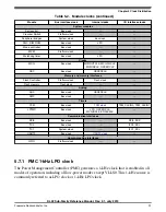
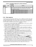
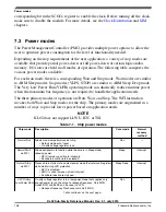


Table 6-2. Flash Option Register (FTFA_FOPT) bit definitions
(continued)
Bit
Num
Field
Value
Definition
4,0
LPBOOT
Controls the reset value of OUTDIV1 value in SIM_CLKDIV1 register. Larger divide value
selections produce lower average power consumption during POR, VLLSx recoveries and
reset sequencing and after reset exit. The recovery times are also extended if the
FAST_INIT option is not selected.
00
Core and system clock divider (OUTDIV1) is 0x7 (divide by 8).
01
Core and system clock divider (OUTDIV1) is 0x3 (divide by 4).
10
Core and system clock divider (OUTDIV1) is 0x1 (divide by 2).
11
Core and system clock divider (OUTDIV1) is 0x0 (divide by 1).
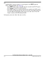
6.3.3 Boot sequence
At power up, the on-chip regulator holds the system in a POR state until the input supply
exceeds the POR threshold. The system continues to be held in this static state until the
internally regulated supplies have reached a safe operating voltage as determined by the
LVD. The Reset Controller logic then controls a sequence to exit reset.
1. A system reset is held on internal logic, the RESET_b pin is driven out low, and the
MCG is enabled in its default clocking mode.
2. Required clocks are enabled (system clock, flash clock, and any bus clocks that do
not have clock gate control reset to disabled).
3. The system reset on internal logic continues to be held, but the Flash Controller is
released from reset and begins initialization operation while the Reset Control logic
continues to drive the RESET_b pin out low.
4. Early in reset sequencing, the NVM option byte is read and stored to the FOPT
register of the Flash Memory module (FTFA_FOPT). If the bits associated with
FTFA_FOPT[LPBOOT] are programmed for an alternate clock divider reset value,
the system/core clock is switched to a slower clock speed. If
FTFA_FOPT[FAST_INIT] is programmed clear, the flash initialization switches to
slower clock resulting longer recovery times.
5. When flash Initialization completes, the RESET_b pin is released. If RESET_b
continues to be asserted (an indication of a slow rise time on the RESET_b pin or
external drive in low), the system continues to be held in reset. Once the RESET_b
pin is detected high, the core clock is enabled and the system is released from reset.
6. When the system exits reset, the processor sets up the stack, program counter (PC),
and link register (LR). The processor reads the start SP (SP_main) from vector-table
offset 0. The core reads the start PC from vector-table offset 4. LR is set to
Chapter 6 Reset and Boot
KL02 Sub-Family Reference Manual, Rev. 2.1, July 2013
Freescale Semiconductor, Inc.
103
Содержание KKL02Z32CAF4R
Страница 2: ...KL02 Sub Family Reference Manual Rev 2 1 July 2013 2 Freescale Semiconductor Inc...
Страница 24: ...KL02 Sub Family Reference Manual Rev 2 1 July 2013 24 Freescale Semiconductor Inc...
Страница 36: ...Orderable part numbers KL02 Sub Family Reference Manual Rev 2 1 July 2013 36 Freescale Semiconductor Inc...
Страница 76: ...Human machine interfaces HMI KL02 Sub Family Reference Manual Rev 2 1 July 2013 76 Freescale Semiconductor Inc...
Страница 94: ...Module clocks KL02 Sub Family Reference Manual Rev 2 1 July 2013 94 Freescale Semiconductor Inc...
Страница 142: ...Functional description KL02 Sub Family Reference Manual Rev 2 1 July 2013 142 Freescale Semiconductor Inc...
Страница 188: ...Memory map and register descriptions KL02 Sub Family Reference Manual Rev 2 1 July 2013 188 Freescale Semiconductor Inc...
Страница 214: ...Application information KL02 Sub Family Reference Manual Rev 2 1 July 2013 214 Freescale Semiconductor Inc...
Страница 222: ...Memory map register descriptions KL02 Sub Family Reference Manual Rev 2 1 July 2013 222 Freescale Semiconductor Inc...
Страница 256: ...Memory map and register definition KL02 Sub Family Reference Manual Rev 2 1 July 2013 256 Freescale Semiconductor Inc...
Страница 300: ...Functional description KL02 Sub Family Reference Manual Rev 2 1 July 2013 300 Freescale Semiconductor Inc...
Страница 532: ...Functional description KL02 Sub Family Reference Manual Rev 2 1 July 2013 532 Freescale Semiconductor Inc...
Страница 534: ...KL02 Sub Family Reference Manual Rev 2 1 July 2013 534 Freescale Semiconductor Inc...


