


24.4.10 Flash Command Description
This section describes all flash commands that can be launched by a command write
sequence. The flash memory module sets the FSTAT[ACCERR] bit and aborts the
command execution if any of the following illegal conditions occur:
• There is an unrecognized command code in the FCCOB FCMD field.
• There is an error in a FCCOB field for the specific commands. Refer to the error
handling table provided for each command.
Ensure that the ACCERR and FPVIOL bits in the FSTAT register are cleared prior to
starting the command write sequence. As described in
Launch the Command by Clearing
, a new command cannot be launched while these error flags are set.
Do not attempt to read a flash block while the flash memory module is running a
command (CCIF = 0) on that same block. The flash memory module may return invalid
data to the MCU with the collision error flag (FSTAT[RDCOLERR]) set.
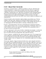
CAUTION
Flash data must be in the erased state before being
programmed. Cumulative programming of bits (adding more
zeros) is not allowed.
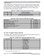
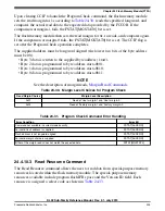
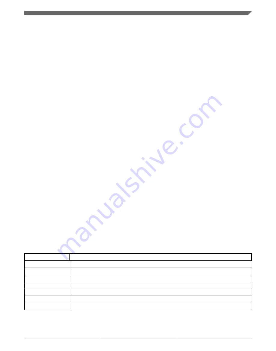
24.4.10.1 Read 1s Section Command
The Read 1s Section command checks if a section of program flash memory is erased to
the specified read margin level. The Read 1s Section command defines the starting
address and the number of longwords to be verified.
Table 24-26. Read 1s Section Command FCCOB Requirements
FCCOB Number
FCCOB Contents [7:0]
0
0x01 (RD1SEC)
1
Flash address [23:16] of the first longword to be verified
2
Flash address [15:8] of the first longword to be verified
3
Flash address [7:0]
of the first longword to be verified
4
Number of longwords to be verified [15:8]
5
Number of longwords to be verified [7:0]
6
Read-1 Margin Choice
1. Must be longword aligned (Flash address [1:0] = 00).
Chapter 24 Flash Memory Module (FTFA)
KL02 Sub-Family Reference Manual, Rev. 2.1, July 2013
Freescale Semiconductor, Inc.
323
Содержание KKL02Z32CAF4R
Страница 2: ...KL02 Sub Family Reference Manual Rev 2 1 July 2013 2 Freescale Semiconductor Inc...
Страница 24: ...KL02 Sub Family Reference Manual Rev 2 1 July 2013 24 Freescale Semiconductor Inc...
Страница 36: ...Orderable part numbers KL02 Sub Family Reference Manual Rev 2 1 July 2013 36 Freescale Semiconductor Inc...
Страница 76: ...Human machine interfaces HMI KL02 Sub Family Reference Manual Rev 2 1 July 2013 76 Freescale Semiconductor Inc...
Страница 94: ...Module clocks KL02 Sub Family Reference Manual Rev 2 1 July 2013 94 Freescale Semiconductor Inc...
Страница 142: ...Functional description KL02 Sub Family Reference Manual Rev 2 1 July 2013 142 Freescale Semiconductor Inc...
Страница 188: ...Memory map and register descriptions KL02 Sub Family Reference Manual Rev 2 1 July 2013 188 Freescale Semiconductor Inc...
Страница 214: ...Application information KL02 Sub Family Reference Manual Rev 2 1 July 2013 214 Freescale Semiconductor Inc...
Страница 222: ...Memory map register descriptions KL02 Sub Family Reference Manual Rev 2 1 July 2013 222 Freescale Semiconductor Inc...
Страница 256: ...Memory map and register definition KL02 Sub Family Reference Manual Rev 2 1 July 2013 256 Freescale Semiconductor Inc...
Страница 300: ...Functional description KL02 Sub Family Reference Manual Rev 2 1 July 2013 300 Freescale Semiconductor Inc...
Страница 532: ...Functional description KL02 Sub Family Reference Manual Rev 2 1 July 2013 532 Freescale Semiconductor Inc...
Страница 534: ...KL02 Sub Family Reference Manual Rev 2 1 July 2013 534 Freescale Semiconductor Inc...


