


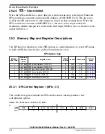


29.1.3 Block diagrams
This section includes block diagrams showing SPI system connections, the internal
organization of the SPI module, and the SPI clock dividers that control the master mode
bit rate.
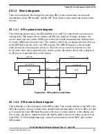
29.1.3.1 SPI system block diagram
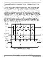
The following figure shows the SPI modules of two MCUs connected in a master-slave
arrangement. The master device initiates all SPI data transfers. During a transfer, the
master shifts data out (on the MOSI pin) to the slave while simultaneously shifting data
in (on the MISO pin) from the slave. The transfer effectively exchanges the data that was
in the SPI shift registers of the two SPI systems. The SPSCK signal is a clock output
from the master and an input to the slave. The slave device must be selected by a low
level on the slave select input (SS pin). In this system, the master device has configured
its SS pin as an optional slave select output.
SPI SHIFTER
MASTER
8 BITS
CLOCK
GENERATOR
MOSI
MISO
MISO
MOSI
SPSCK
SPSCK
SS
SS
SLAVE
SPI SHIFTER
8 BITS
Figure 29-1. SPI system connections
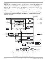
29.1.3.2 SPI module block diagram
The following is a block diagram of the SPI module. The central element of the SPI is the
SPI shift register. Data is written to the double-buffered transmitter (write to SPIx_D) and
gets transferred to the SPI Shift Register at the start of a data transfer. After shifting in 8
bits of data, the data is transferred into the double-buffered receiver where it can be read
from SPIx_D. Pin multiplexing logic controls connections between MCU pins and the
SPI module.
Chapter 29 Serial Peripheral Interface (SPI)
KL02 Sub-Family Reference Manual, Rev. 2.1, July 2013
Freescale Semiconductor, Inc.
445
Содержание KKL02Z32CAF4R
Страница 2: ...KL02 Sub Family Reference Manual Rev 2 1 July 2013 2 Freescale Semiconductor Inc...
Страница 24: ...KL02 Sub Family Reference Manual Rev 2 1 July 2013 24 Freescale Semiconductor Inc...
Страница 36: ...Orderable part numbers KL02 Sub Family Reference Manual Rev 2 1 July 2013 36 Freescale Semiconductor Inc...
Страница 76: ...Human machine interfaces HMI KL02 Sub Family Reference Manual Rev 2 1 July 2013 76 Freescale Semiconductor Inc...
Страница 94: ...Module clocks KL02 Sub Family Reference Manual Rev 2 1 July 2013 94 Freescale Semiconductor Inc...
Страница 142: ...Functional description KL02 Sub Family Reference Manual Rev 2 1 July 2013 142 Freescale Semiconductor Inc...
Страница 188: ...Memory map and register descriptions KL02 Sub Family Reference Manual Rev 2 1 July 2013 188 Freescale Semiconductor Inc...
Страница 214: ...Application information KL02 Sub Family Reference Manual Rev 2 1 July 2013 214 Freescale Semiconductor Inc...
Страница 222: ...Memory map register descriptions KL02 Sub Family Reference Manual Rev 2 1 July 2013 222 Freescale Semiconductor Inc...
Страница 256: ...Memory map and register definition KL02 Sub Family Reference Manual Rev 2 1 July 2013 256 Freescale Semiconductor Inc...
Страница 300: ...Functional description KL02 Sub Family Reference Manual Rev 2 1 July 2013 300 Freescale Semiconductor Inc...
Страница 532: ...Functional description KL02 Sub Family Reference Manual Rev 2 1 July 2013 532 Freescale Semiconductor Inc...
Страница 534: ...KL02 Sub Family Reference Manual Rev 2 1 July 2013 534 Freescale Semiconductor Inc...


