


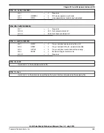

29.4 Functional description
This section provides the functional description of the module.
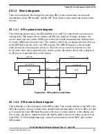
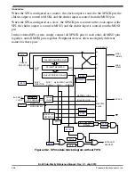
29.4.1 General
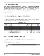
The SPI system is enabled by setting the SPI enable (SPE) bit in SPI Control Register 1.
While C1[SPE] is set, the four associated SPI port pins are dedicated to the SPI function
as:
• Slave select (SS)
• Serial clock (SPSCK)
• Master out/slave in (MOSI)
• Master in/slave out (MISO)
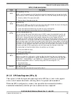
An SPI transfer is initiated in the master SPI device by reading the SPI status register
(SPIx_S) when S[SPTEF] = 1 and then writing data to the transmit data buffer (write to
SPIxD ). When a transfer is complete, received data is moved into the receive data buffer.
The SPIxD register acts as the SPI receive data buffer for reads and as the SPI transmit
data buffer for writes.
The Clock Phase Control (CPHA) and Clock Polarity Control (CPOL) bits in the SPI
Control Register 1 (SPIx_C1) select one of four possible clock formats to be used by the
SPI system. The CPOL bit simply selects a non-inverted or inverted clock. C1[CPHA] is
used to accommodate two fundamentally different protocols by sampling data on odd
numbered SPSCK edges or on even numbered SPSCK edges.
The SPI can be configured to operate as a master or as a slave. When the MSTR bit in
SPI Control Register 1 is set, master mode is selected; when C1[MSTR] is clear, slave
mode is selected.
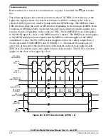
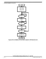
29.4.2 Master mode
The SPI operates in master mode when C1[MSTR] is set. Only a master SPI module can
initiate transmissions. A transmission begins by reading the SPIx_S register while
S[SPTEF] = 1 and writing to the master SPI data registers. If the shift register is empty,
the byte immediately transfers to the shift register. The data begins shifting out on the
MOSI pin under the control of the serial clock.
Chapter 29 Serial Peripheral Interface (SPI)
KL02 Sub-Family Reference Manual, Rev. 2.1, July 2013
Freescale Semiconductor, Inc.
455
Содержание KKL02Z32CAF4R
Страница 2: ...KL02 Sub Family Reference Manual Rev 2 1 July 2013 2 Freescale Semiconductor Inc...
Страница 24: ...KL02 Sub Family Reference Manual Rev 2 1 July 2013 24 Freescale Semiconductor Inc...
Страница 36: ...Orderable part numbers KL02 Sub Family Reference Manual Rev 2 1 July 2013 36 Freescale Semiconductor Inc...
Страница 76: ...Human machine interfaces HMI KL02 Sub Family Reference Manual Rev 2 1 July 2013 76 Freescale Semiconductor Inc...
Страница 94: ...Module clocks KL02 Sub Family Reference Manual Rev 2 1 July 2013 94 Freescale Semiconductor Inc...
Страница 142: ...Functional description KL02 Sub Family Reference Manual Rev 2 1 July 2013 142 Freescale Semiconductor Inc...
Страница 188: ...Memory map and register descriptions KL02 Sub Family Reference Manual Rev 2 1 July 2013 188 Freescale Semiconductor Inc...
Страница 214: ...Application information KL02 Sub Family Reference Manual Rev 2 1 July 2013 214 Freescale Semiconductor Inc...
Страница 222: ...Memory map register descriptions KL02 Sub Family Reference Manual Rev 2 1 July 2013 222 Freescale Semiconductor Inc...
Страница 256: ...Memory map and register definition KL02 Sub Family Reference Manual Rev 2 1 July 2013 256 Freescale Semiconductor Inc...
Страница 300: ...Functional description KL02 Sub Family Reference Manual Rev 2 1 July 2013 300 Freescale Semiconductor Inc...
Страница 532: ...Functional description KL02 Sub Family Reference Manual Rev 2 1 July 2013 532 Freescale Semiconductor Inc...
Страница 534: ...KL02 Sub Family Reference Manual Rev 2 1 July 2013 534 Freescale Semiconductor Inc...


