Freescale Semiconductor KKL02Z32CAF4R Скачать руководство пользователя страница 109

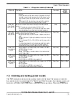
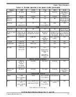
Table 7-1. Chip power modes (continued)

Chip mode

Description

Core mode

Normal

recovery

method

• LVD off
• In BLPI clock mode, only the fast internal reference oscillator is

available to provide a low power nominal 4 MHz source for the
core with the nominal bus and flash clock required to be <800
kHz

• Alternatively, BLPE clock mode can be used with an external

clock or the crystal oscillator providing the clock source.

VLPW (Very

Low-Power

Wait) -via WFI

Same as VLPR but with the core in Sleep mode to further reduce
power.

• NVIC remains sensitive to interrupts (FCLK = ON).
• On-chip voltage regulator is in a low-power mode that supplies

only enough power to run the chip at a reduced frequency.

Sleep

Interrupt

VLPS (Very

Low-Power

Stop)-via WFI

Places chip in static state with LVD operation off. Lowest power mode
with ADC and pin interrupts functional.

• Peripheral clocks are stopped, but OSC, LPTMR, CMP can be

used.

• TPM and UART can optionally be enabled if their clock source is

enabled.

• NVIC is disabled (FCLK = OFF); AWIC is used to wake up from

interrupt.

• On-chip voltage regulator is in a low-power mode that supplies

only enough power to run the chip at a reduced frequency.

• All SRAM is operating (content retained and I/O states held).
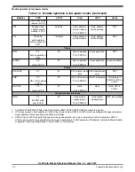
Sleep Deep

Interrupt

VLLS3 (Very

Low-Leakage

Stop3)

• Most peripherals are disabled (with clocks stopped), but OSC,

LPTMR, CMP can be used.

• NVIC is disabled.
• SRAM_U and SRAM_L remain powered on (content retained

and I/O states held).

Sleep Deep

Wake-up Reset

VLLS1 (Very

Low-Leakage

Stop1)

• Most peripherals are disabled (with clocks stopped), but OSC,

LPTMR, CMP can be used.

• NVIC is disabled.
• All of SRAM_U and SRAM_L are powered off.

Sleep Deep

Wake-up Reset

VLLS0 (Very

Low-Leakage

Stop 0)

• Most peripherals are disabled (with clocks stopped), but LPTMR

can be used.

• NVIC is disabled.
• All of SRAM_U and SRAM_L are powered off.
• LPO disabled, optional POR brown-out detection

Sleep Deep

Wake-up Reset

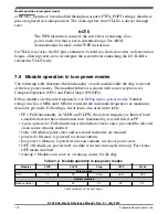
7.4 Entering and exiting power modes

The WFI instruction invokes wait and stop modes for the chip. The processor exits the
low-power mode via an interrupt. For VLLS3 and VLLS1 modes, the wakeup sources are
limited to LPTMR, CMP,NMI_b pin, or RESET_b pin assertions. When the NMI_b pin

Chapter 7 Power Management

KL02 Sub-Family Reference Manual, Rev. 2.1, July 2013

Freescale Semiconductor, Inc.

109

Содержание KKL02Z32CAF4R

Страница 1: ...KL02 Sub Family Reference Manual Supports MKL02Z32CAF4R and KKL02Z32CAF4R Document Number KL02P20M48SF0RM Rev 2 1 July 2013...

Страница 2: ...KL02 Sub Family Reference Manual Rev 2 1 July 2013 2 Freescale Semiconductor Inc...

Страница 3: ...family introduction 30 2 4 Module functional categories 31 2 4 1 ARM Cortex M0 core modules 32 2 4 2 System modules 32 2 4 3 Memories and memory interfaces 33 2 4 4 Clocks 33 2 4 5 Security and integ...

Страница 4: ...1 SIM configuration 46 3 4 2 System mode controller SMC configuration 47 3 4 3 PMC configuration 48 3 4 4 MCM configuration 48 3 4 5 Crossbar light switch configuration 49 3 4 6 Peripheral bridge con...

Страница 5: ...3 Chapter 4 Memory Map 4 1 Introduction 77 4 2 System memory map 77 4 3 Flash memory map 78 4 3 1 Alternate non volatile IRC user trim description 78 4 4 SRAM memory map 79 4 5 Bit Manipulation Engine...

Страница 6: ...ule clocks 90 5 7 1 PMC 1 kHz LPO clock 91 5 7 2 COP clocking 91 5 7 3 LPTMR clocking 92 5 7 4 TPM clocking 92 5 7 5 UART clocking 93 Chapter 6 Reset and Boot 6 1 Introduction 95 6 2 Reset 95 6 2 1 Po...

Страница 7: ...urity 8 1 Introduction 113 8 2 Flash security 113 8 3 Security interactions with other modules 113 8 3 1 Security interactions with Debug 114 Chapter 9 Debug 9 1 Introduction 115 9 2 Debug port pin de...

Страница 8: ...1 Core modules 127 10 4 2 System modules 127 10 4 3 Clock modules 128 10 4 4 Memories and memory interfaces 128 10 4 5 Analog 128 10 4 6 Timer Modules 129 10 4 7 Communication interfaces 129 10 4 8 Hu...

Страница 9: ...ister 7 SIM_SOPT7 148 12 2 5 System Device Identification Register SIM_SDID 149 12 2 6 System Clock Gating Control Register 4 SIM_SCGC4 151 12 2 7 System Clock Gating Control Register 5 SIM_SCGC5 153...

Страница 10: ...es 175 13 4 4 Wait modes 176 13 4 5 Stop modes 177 13 4 6 Debug in low power modes 179 Chapter 14 Power Management Controller PMC 14 1 Introduction 181 14 2 Features 181 14 3 Low voltage detect LVD sy...

Страница 11: ...description 197 16 3 Memory map and register definition 198 16 4 Functional description 198 16 4 1 BME decorated stores 198 16 4 2 BME decorated loads 205 16 4 3 Additional details on decorated addre...

Страница 12: ...y Map 251 Chapter 19 Crossbar Switch Lite AXBS Lite 19 1 Introduction 257 19 1 1 Features 257 19 2 Memory Map Register Definition 257 19 3 Functional Description 258 19 3 1 General operation 258 19 3...

Страница 13: ...21 3 7 MCG Status and Control Register MCG_SC 272 21 3 8 MCG Auto Trim Compare Value High Register MCG_ATCVH 274 21 3 9 MCG Auto Trim Compare Value Low Register MCG_ATCVL 274 21 4 Functional Descripti...

Страница 14: ...ional Description 292 22 8 1 OSC Module States 292 22 8 2 OSC Module Modes 294 22 8 3 Counter 295 22 8 4 Reference Clock Pin Requirements 295 22 9 Reset 296 22 10 Low Power Modes Operation 296 22 11 I...

Страница 15: ...Protection 315 24 4 2 Interrupts 315 24 4 3 Flash Operation in Low Power Modes 316 24 4 4 Functional Modes of Operation 317 24 4 5 Flash Reads and Ignored Writes 317 24 4 6 Read While Write RWW 317 2...

Страница 16: ...de General Calibration Value Register ADCx_CLPD 356 25 3 11 ADC Plus Side General Calibration Value Register ADCx_CLPS 356 25 3 12 ADC Plus Side General Calibration Value Register ADCx_CLP4 357 25 3 1...

Страница 17: ...3 6 bit DAC key features 384 26 4 ANMUX key features 384 26 5 CMP DAC and ANMUX diagram 385 26 6 CMP block diagram 386 26 7 Memory map register definitions 387 26 7 1 CMP Control Register 0 CMPx_CR0 3...

Страница 18: ...2 Features 409 27 1 3 Modes of Operation 410 27 1 4 Block Diagram 410 27 2 TPM Signal Descriptions 411 27 2 1 TPM_EXTCLK TPM External Clock 411 27 2 2 TPM_CHn TPM Channel n I O Pin 412 27 3 Memory Map...

Страница 19: ...8 1 2 Modes of operation 433 28 2 LPTMR signal descriptions 434 28 2 1 Detailed signal descriptions 434 28 3 Memory map and register definition 434 28 3 1 Low Power Timer Control Status Register LPTMR...

Страница 20: ...Slave Data Out 447 29 2 4 SS Slave Select 447 29 3 Memory Map and Register Descriptions 448 29 3 1 SPI Control Register 1 SPIx_C1 448 29 3 2 SPI Control Register 2 SPIx_C2 450 29 3 3 SPI Baud Rate Reg...

Страница 21: ...tions 473 30 3 Memory map and register descriptions 473 30 3 1 I2C Address Register 1 I2Cx_A1 474 30 3 2 I2C Frequency Divider register I2Cx_F 475 30 3 3 I2C Control Register 1 I2Cx_C1 476 30 3 4 I2C...

Страница 22: ...UART Control Register 2 UARTx_C2 502 31 2 5 UART Status Register 1 UARTx_S1 503 31 2 6 UART Status Register 2 UARTx_S2 505 31 2 7 UART Control Register 3 UARTx_C3 507 31 2 8 UART Data Register UARTx_...

Страница 23: ...ta Input Register GPIOx_PDIR 526 32 2 6 Port Data Direction Register GPIOx_PDDR 526 32 3 FGPIO memory map and register definition 527 32 3 1 Port Data Output Register FGPIOx_PDOR 528 32 3 2 Port Set O...

Страница 24: ...KL02 Sub Family Reference Manual Rev 2 1 July 2013 24 Freescale Semiconductor Inc...

Страница 25: ...identify different numbering systems This suffix Identifies a b Binary number For example the binary equivalent of the number 5 is written 101b In some cases binary numbers are shown with the prefix...

Страница 26: ...4 XAD 7 0 Numbers in brackets and separated by a colon represent either A subset of a register s named field For example REVNO 6 4 refers to bits 6 4 that are part of the COREREV field that occupies b...

Страница 27: ...ntegration This scalability allows developers to standardize on the Kinetis L Series for their end product platforms maximising hardware and software reuse and reducing time to market Features common...

Страница 28: ...MCUs KL2x Family KL1x Family KL0x Family KL3x Family Family Program Flash Packages Key Features Low power Mixed signal USB Segment LCD KL4x Family 8 32KB 32 256KB 32 256KB 64 256KB 128 256KB 16 48pin...

Страница 29: ...l registers eliminating traditional methods where the core would need to perform read modify write operations Up to 4 channel DMA for peripheral and memory servicing with minimal CPU intervention feat...

Страница 30: ...lity safety and security Internal watchdog with independent clock source Timing and control Powerful timer modules which support general purpose PWM and motor control functions Periodic Interrupt Time...

Страница 31: ...MHz from single cycle access memories 48 MHz CPU frequency System System integration module Power management and mode controllers Multiple power modes available based on run wait stop and power down...

Страница 32: ...detect asynchronous wake up events in stop modes and signal to clock control logic to resume system clocking After clock restart the NVIC observes the pending interrupt and performs the normal interr...

Страница 33: ...es and memory interfaces The following memories and memory interfaces are available on this device Table 2 4 Memories and memory interfaces Module Description Flash memory Program flash memory up to 3...

Страница 34: ...imer modules are available on this device Table 2 8 Timer modules Module Description Timer PWM module TPM Selectable TPM clock mode Prescaler divide by 1 2 4 8 16 32 64 or 128 16 bit free running coun...

Страница 35: ...aces The following human machine interfaces HMI are available on this device Table 2 10 HMI modules Module Description General purpose input output GPIO Some general purpose input or output GPIO pins...

Страница 36: ...Orderable part numbers KL02 Sub Family Reference Manual Rev 2 1 July 2013 36 Freescale Semiconductor Inc...

Страница 37: ...module to module interconnections for this device Table 3 1 Module to module interconnects Peripheral Signal to Peripheral Use Case Control Comment TPM1 CH0F CH1F to ADC Trigger ADC Triggering A AND...

Страница 38: ...TPM1 CH0 Input capture SOPT4_TPM1CH0SR C CMP0 CMP0_OUT to UART0_RX IR interface SOPT5_UART0RXSR C LPTMR Hardware trigger to CMPx Low power triggering of the comparator CMP_CR1 TRIGM LPTMR Hardware tr...

Страница 39: ...this option for the best ADC operation 3 3 Core modules 3 3 1 ARM Cortex M0 core configuration This section summarizes how the module has been configured in the chip Full documentation for this module...

Страница 40: ...points BKPT 2 Implements 2 breakpoints Debug Support DBG 1 Present Halt Event Support HALTEV 1 Present I O Port IOP 1 Present Implements single cycle ld st accesses to special address space IRQ Mask E...

Страница 41: ...port bus interfacing to the GPIO with 1 cycle loads and stores 3 3 1 3 System tick timer The CLKSOURCE field in SysTick Control and Status register selects either the core clock when CLKSOURCE 1 or a...

Страница 42: ...r management Power management Private peripheral bus PPB ARM Cortex M0 core ARM Cortex M0 core 3 3 2 1 Interrupt priority levels This device supports four priority levels for interrupts Therefore in t...

Страница 43: ...tors 0x0000_0000 0 ARM core Initial stack pointer 0x0000_0004 1 ARM core Initial program counter 0x0000_0008 2 ARM core Non maskable interrupt NMI 0x0000_000C 3 ARM core Hard fault 0x0000_0010 4 0x000...

Страница 44: ...0x0000_0090 36 20 5 0x0000_0094 37 21 5 0x0000_0098 38 22 5 0x0000_009C 39 23 5 0x0000_00A0 40 24 6 0x0000_00A4 41 25 6 0x0000_00A8 42 26 6 0x0000_00AC 43 27 6 MCG 0x0000_00B0 44 28 7 LPTMR0 0x0000_00...

Страница 45: ...Therefore the following field locations are used to configure the SPI0 interrupts NVICIPR2 23 22 3 3 3 Asynchronous wake up interrupt controller AWIC configuration This section summarizes how the mod...

Страница 46: ...tional in Stop mode Pin interrupts Port control module any enabled pin interrupt is capable of waking the system ADC The ADC is functional when using internal clock source CMP0 Interrupt in normal or...

Страница 47: ...gured in the chip For a comprehensive description of the module itself see the module s dedicated chapter Power Management Controller PMC Register access Peripheral bridge System Mode Controller SMC R...

Страница 48: ...f the module itself see the module s dedicated chapter Register access Power Management Controller PMC Peripheral bridge Module signals System Mode Controller SMC Figure 3 6 PMC configuration Table 3...

Страница 49: ...e Full description Miscellaneous control module MCM MCM System memory map System memory map Clocking Clock distribution Power management Power management Private peripheral bus PPB ARM Cortex M0 core...

Страница 50: ...k distribution Crossbar switch master ARM Cortex M0 core ARM Cortex M0 core Crossbar switch slave Flash memory controller Flash memory controller Crossbar switch slave SRAM controller SRAM configurati...

Страница 51: ...ossbar switch Figure 3 9 Peripheral bridge configuration Table 3 16 Reference links to related information Topic Related module Reference Full description Peripheral bridge AIPS Lite Peripheral bridge...

Страница 52: ...and the bus clock 3 4 7 2 COP watchdog operation The COP watchdog is intended to force a system reset when the application software fails to execute as expected To prevent a system reset from the COP...

Страница 53: ...s 32 ms 0 10 1 kHz N A 28 cycles 256 ms 0 11 1 kHz N A 210 cycles 1024 ms 1 01 Bus 6 144 cycles 213 cycles 1 10 Bus 49 152 cycles 216 cycles 1 11 Bus 196 608 cycles 218 cycles After the bus clock sour...

Страница 54: ...nabled as for any reset 3 4 7 3 Clock gating This family of devices includes clock gating control for each peripheral that is the clock to each peripheral can explicitly be gated on or off using clock...

Страница 55: ...configuration This section summarizes how the module has been configured in the chip For a comprehensive description of the module itself see the module s dedicated chapter Signal multiplexing Regist...

Страница 56: ...ces 3 6 1 Flash memory configuration This section summarizes how the module has been configured in the chip For a comprehensive description of the module itself see the module s dedicated chapter Regi...

Страница 57: ...memory map Flash Flash configuration field Flash base address Flash memory base address Registers Figure 3 14 Flash memory map The on chip flash memory is implemented in a portion of the allocated Fla...

Страница 58: ...er to customize the operation of the MCU at boot time See FOPT boot options for details of its definition 3 6 2 Flash memory controller configuration This section summarizes how the module has been co...

Страница 59: ...SRAM configuration Table 3 24 Reference links to related information Topic Related module Reference Full description SRAM SRAM System memory map System memory map Clocking Clock distribution ARM Cort...

Страница 60: ...e space after this beginning address Valid address ranges for SRAM_L and SRAM_U are then defined as SRAM_L 0x2000_0000 SRAM_size 4 to 0x1FFF_FFFF SRAM_U 0x2000_0000 to 0x2000_0000 SRAM_size 3 4 1 This...

Страница 61: ...ister access 12 bit SAR ADC Peripheral bus controller 0 Other peripherals Figure 3 18 12 bit SAR ADC configuration Table 3 26 Reference links to related information Topic Related module Reference Full...

Страница 62: ...0 00001 AD1 Reserved ADC0_SE1 00010 AD2 Reserved ADC0_SE2 00011 AD3 Reserved ADC0_SE3 00100 AD4 Reserved ADC0_SE4 00101 AD5 Reserved Reserved 00110 AD6 Reserved Reserved 00111 AD7 Reserved Reserved 01...

Страница 63: ...VSS This device contains separate VREFH and VREFL pins on 32 pin and higher devices These pins are internally connected to VDD and VSS respectively on packages less than 32 pin 3 7 1 4 Alternate cloc...

Страница 64: ...nel assignment table for a summary of CMP input connections for this device The CMP also includes one 6 bit DAC with a 64 tap resistor ladder network which provides a selectable voltage reference for...

Страница 65: ...FH Vin1 input When using VREFH any ADC conversion using this same reference at the same time is negatively impacted VDD Vin2 input 3 7 2 4 CMP trigger mode The CMP and 6 bit DAC sub block supports tri...

Страница 66: ...module has been configured in the chip For a comprehensive description of the module itself see the module s dedicated chapter Signal multiplexing Module signals Register access TPM Peripheral bus con...

Страница 67: ...be selected from OSCERCLK MCGIRCLK or MCGFLLCLK The selected source is controlled by SIM_SOPT2 TPMSRC Each TPM also supports an external clock mode TPM_SC CMOD 1x in which the counter increments afte...

Страница 68: ...configured as the global time when this option is enabled 3 8 1 5 TPM interrupts The TPM has multiple sources of interrupt However these sources are OR d together to generate a single interrupt reques...

Страница 69: ...includes a 2N prescaler real time interrupt mode or glitch filter pulse accumulator mode The LPTMR can be clocked from the internal reference clock the internal 1 kHz LPO OSCERCLK or an external 32 7...

Страница 70: ...itch filter clock number Chip clock 00 0 MCGIRCLK internal reference clock not available in VLLS modes 01 1 LPO 1 kHz clock not available in VLLS0 mode 10 2 ERCLK32K not available in VLLS0 mode when u...

Страница 71: ...s device contains one SPI module that supports 8 bit data length SPI0 is clocked on the bus clock The SPI can operate in VLPS mode When the SPI is operating in VLPS mode it will operate as a slave SPI...

Страница 72: ...en the package pins associated with IIC have their mux select configured for IIC operation the pins SCL and SDA are driven in a pseudo open drain configuration The digital glitch filter implemented in...

Страница 73: ...erview The UART0 module supports basic UART x4 to x32 oversampling of baud rate This module supports LIN slave operation The module can remain functional in VLPS mode provided the clock it is using re...

Страница 74: ...2 and PTA13 with high current drive capability These pins can be used to drive LED or power MOSFET directly The high drive capability applies to all functions which are multiplexed on these pins UART...

Страница 75: ...reset Disabled Disabled Pin mux control Yes Yes Pin mux at reset PTA0 PTA2 ALT3 Others ALT0 PTB5 ALT3 Others ALT0 Lock bit No No Interrupt request PTA0 PTA1 PTA7 PTA10 PTA11 PTA12 only PTB0 PTB1 PTB2...

Страница 76: ...Human machine interfaces HMI KL02 Sub Family Reference Manual Rev 2 1 July 2013 76 Freescale Semiconductor Inc...

Страница 77: ...ore 0x2000_0000 0x2000_0BFF2 SRAM_U Upper SRAM Cortex M0 core 0x2000_0C00 0x3FFF_FFFF Reserved 0x4000_0000 0x4007_FFFF AIPS Peripherals Cortex M0 core 0x4008_0000 0x400F_EFFF Reserved 0x400F_F000 0x40...

Страница 78: ...fied in System memory map Flash Flash configuration field Flash base address Flash memory base address Registers Figure 4 1 Flash memory map The on chip flash memory is implemented in a portion of the...

Страница 79: ...ace By combining the basic load and store instruction support in the Cortex M instruction set architecture with the concept of decorated storage provided by the BME the resulting implementation provid...

Страница 80: ...Accessing an address that is not implemented in the peripheral results in a transfer error termination 4 6 1 Read after write sequence and required serialization of memory operations In some situation...

Страница 81: ...01_1000 17 0x4001_2000 18 0x4001_3000 19 0x4001_4000 20 0x4001_5000 21 0x4001_6000 22 0x4001_7000 23 0x4001_8000 24 0x4001_9000 25 0x4001_A000 26 0x4001_B000 27 0x4001_C000 28 0x4001_D000 29 0x4001_E0...

Страница 82: ...ADC 0 0x4003_C000 60 0x4003_D000 61 0x4003_E000 62 0x4003_F000 63 0x4004_0000 64 Low power timer LPTMR 0x4004_1000 65 0x4004_2000 66 0x4004_3000 67 0x4004_4000 68 0x4004_5000 69 0x4004_6000 70 0x4004_...

Страница 83: ...i purpose clock generator MCG 0x4006_5000 101 System oscillator OSC 0x4006_6000 102 I2C 0 0x4006_7000 103 I2C 1 0x4006_8000 104 0x4006_9000 105 0x4006_A000 106 UART 0 0x4006_B000 107 0x4006_C000 108 0...

Страница 84: ...s architecture and provides access to select processor local modules These resources are only accessible from the core other system masters do not have access to them Table 4 3 PPB memory map System 3...

Страница 85: ...lectable clock input 5 2 Programming model The selection and multiplexing of system clock sources is controlled and programmed via the MCG module The setting of clock dividers and module clock gating...

Страница 86: ...IV Core clock platform clock and system clock Figure 5 1 Clocking diagram 5 4 Clock definitions The following table describes the clocks in the previous block diagram Clock name Description Core clock...

Страница 87: ...The following table provides more information regarding the on chip clocks Table 5 1 Clock summary Clock name Run mode clock frequency VLPR mode clock frequency Clock source Clock is disabled when MCG...

Страница 88: ...z ERCLK32K 30 40 kHz 30 40 kHz System OSC System OSC s OSC_CR ERCLKEN cleared or VLLS0 and oscillator not in external clock mode LPO 1 kHz 1 kHz PMC in VLLS0 TPM clock Up to 48 MHz Up to 8 MHz MCGIRCL...

Страница 89: ...ck and flash clock dividers as shown in the table given below FTFA_FOPT 4 0 Core system clock Bus Flash clock Description 00 0x7 divide by 8 0x1 divide by 2 Low power boot 01 0x3 divide by 4 0x1 divid...

Страница 90: ...in a divide by 5 setting 5 6 Clock gating The clock to each module can be individually gated on and off using bits of the SCGCx registers of the SIM module These bits are cleared after any reset which...

Страница 91: ...h clock Analog ADC Bus clock OSCERCLK CMP Bus clock Timers TPM Bus clock TPM clock TPM_CLKIN0 TPM_CLKIN1 LPTMR Bus clock LPO OSCERCLK MCGIRCLK ERCLK32K Communication interfaces SPI0 Bus clock SPI0_SCK...

Страница 92: ...in the following figure NOTE The chosen clock must remain enabled if the LPTMRx is to continue operating in all required low power modes LPTMRx_PSR PCS LPTMRx prescaler glitch filter clock MCGIRCLK OS...

Страница 93: ...UART clocking The UART0 module has a selectable clock as shown in the following figure NOTE The chosen clock must remain enabled if the UART0 is to continue operating in all required low power modes...

Страница 94: ...Module clocks KL02 Sub Family Reference Manual Rev 2 1 July 2013 94 Freescale Semiconductor Inc...

Страница 95: ...Each of the system reset sources has an associated bit in the System Reset Status SRS registers See the Reset Control Module for register details The MCU can exit and reset in functional mode where t...

Страница 96: ...offset 0 Reads the start PC from vector table offset 4 LR is set to 0xFFFF_FFFF The on chip peripheral modules are disabled and the non analog I O pins are initially configured as disabled The pins w...

Страница 97: ...ct memory contents and control MCU system states during supply voltage variations The system consists of a power on reset POR circuit and an LVD circuit with a user selectable trip voltage The LVD sys...

Страница 98: ...can be caused by a failure of an external clock input to a module 6 2 2 6 Software reset SW The SYSRESETREQ field in the NVIC Application Interrupt and Reset Control register can be set to force a sof...

Страница 99: ...POR not VLLS The Chip POR not VLLS reset asserts on POR and LVD reset sources It resets parts of the SMC and SIM It also resets the LPTMR The Chip POR not VLLS reset also causes these resets to occur...

Страница 100: ...pin is driven low by the MCU for at least 128 bus clock cycles and until flash initialization has completed After flash initialization has completed the RESET_b pin is released and the internal Chip R...

Страница 101: ...the boot sequence including sources and options Some configuration information such as clock trim values stored in factory programmed flash locations is autoloaded 6 3 1 Boot sources The CM0 core add...

Страница 102: ...OT setting 1 Fast Initialization The flash has faster recoveries at the expense of higher current during these times 3 RESET_PIN_CFG Enables disables control for the RESET pin 0 RESET_b pin is disable...

Страница 103: ...ock and any bus clocks that do not have clock gate control reset to disabled 3 The system reset on internal logic continues to be held but the Flash Controller is released from reset and begins initia...

Страница 104: ...ion If the NMI_b input is low and the NMI function is enabled in the FOPT register this results in an NMI interrupt The processor executes an Exception Entry and reads the NMI interrupt handler addres...

Страница 105: ...VLP Run mode When configured for PSTOP2 only the core and system clocks are gated and the bus clock remains active The bus masters and bus slaves clocked by the system clock enter Stop mode but the bu...

Страница 106: ...Stop mode also remains functional in Compute Operation including generation of asynchronous interrupts requests When enabling Compute Operation in Run mode module functionality for bus masters and sla...

Страница 107: ...include all of the modes of operation listed below The CPU is in Wait mode The CPU is in Stop mode including the entry sequence The CPU is in Compute Operation including the entry sequence Peripheral...

Страница 108: ...n Wait and Stop The WFI instruction invokes both Wait and Stop modes for the chip The primary modes are augmented in a number of ways to provide lower power based on application needs NOTE KL02 does n...

Страница 109: ...chip voltage regulator is in a low power mode that supplies only enough power to run the chip at a reduced frequency All SRAM is operating content retained and I O states held Sleep Deep Interrupt VL...

Страница 110: ...gs such as 4 MHz and 1 Mbit s represent the maximum frequencies or maximum data rates per mode Following is list of terms also used in the table FF Full functionality In VLPR and VLPW the system frequ...

Страница 111: ...IRC optional OFF Core clock 4 MHz max OFF OFF OFF OFF System clock 4 MHz max OFF in CPO 4 MHz max OFF OFF OFF Bus clock 1 MHz max OFF in CPO 1 MHz max OFF 24 MHz max in PSTOP2 from RUN 1MHz max in PS...

Страница 112: ...e in VLLS1 3 OFF in VLLS0 6 bit DAC FF static in CPO FF static FF in PSTOP2 static static OFF in VLLS0 Human machine interfaces GPIO FF IOPORT write only in CPO FF static output wakeup input FF in PST...

Страница 113: ...xternal accesses debug CPU accesses to the flash are not affected by the status of FTFA_FSEC In the unsecured state all flash commands are available on the programming interfaces either from the debug...

Страница 114: ...the Flash Mass Erase in Progress field of the MDM AP Control register to trigger a mass erase Erase All Blocks command A mass erase via the debugger is allowed even when some memory locations are prot...

Страница 115: ...supported Serial Wire Debug SWD 9 2 Debug port pin descriptions The debug port pins default after POR to their SWD functionality Table 9 1 Serial wire debug pin description Pin name Type Description...

Страница 116: ...remaining less intrusive during a debug session It is important to note that these DAP control and status registers are not memory mapped within the system memory map and are only accessible via the...

Страница 117: ...STAT AP Select SELECT Read Buffer RDBUFF DP Registers 0x00 0x04 0x08 0x0C Data 31 0 A 3 2 RnW DPACC Data 31 0 A 3 2 RnW APACC Debug Port DP Generic See the ARM Debug Interface v5p1 Supplement Figure 9...

Страница 118: ...low the debugger time to re initialize debug IP before the debug session continues The Mode Controller captures this bit logic on entry to VLLSx modes Upon exit from VLLSx modes the Mode Controller wi...

Страница 119: ...ed 1 Mass erase is enabled 6 Backdoor Access Key Enable Indicates if the MCU has the backdoor access key enabled 0 Disabled 1 Enabled 7 LP Enabled Decode of SMC_PMCTRL STOPM field to indicate that VLP...

Страница 120: ...ger to reset the debug logic System POR reset Conversely the debug system is capable of generating system reset using the following mechanism A system reset in the DAP control register which allows th...

Страница 121: ...r is reset on recovery and must be reconfigured once the low power mode is exited Power mode entry logic monitors Debug Power Up and System Power Up signals from the debug port as indications that a d...

Страница 122: ...a In the secure state the debugger still has access to the status register and can determine the current security state of the device In the case of a secure device the debugger has the capability of...

Страница 123: ...Signal multiplexing integration This section summarizes how the module is integrated into the device For a comprehensive description of the module itself see the module s dedicated chapter Register ac...

Страница 124: ...ability PS 1 PTA0 0 Fixed All are read only PE 0 PTA0 and PTA2 1 Yes All GPIOs are configurable DSE 0 No exceptions all DSE are cleared on reset 4 pins are configurable for High Drive PTB0 PTB1 PTA12...

Страница 125: ...the same function to more than one pin 2 To ensure the best signal timing for a given peripheral s interface choose the pins in closest proximity to each other 10 3 Pinout 10 3 1 KL02 signal multiplex...

Страница 126: ...0_SDA UART0_RX B2 PTB5 IRQ_12 NMI_b ADC0_SE1 CMP0_IN1 PTB5 IRQ_12 TPM1_CH1 NMI_b A1 PTA12 IRQ_13 LPTMR0_ALT2 ADC0_SE0 CMP0_IN0 ADC0_SE0 CMP0_IN0 PTA12 IRQ_13 LPTMR0_ALT2 TPM1_CH0 TPM_CLKIN0 A2 PTB13 A...

Страница 127: ...le signal name Description I O SWD_DIO SWD_DIO Serial Wire Debug Data Input Output The SWD_DIO pin is used by an external debug tool for communication and device control This pin is pulled up internal...

Страница 128: ...I XTAL0 XTAL Oscillator output O 10 4 4 Memories and memory interfaces 10 4 5 Analog Table 10 6 ADC0 signal descriptions Chip signal name Module signal name Description I O ADC0_SEn ADn Single Ended A...

Страница 129: ...0 Signal Descriptions Chip signal name Module signal name Description I O LPTMR0_ALT 2 1 LPTMR_ALTn Pulse Counter Input pin I 10 4 7 Communication interfaces Table 10 11 SPI0 signal descriptions Chip...

Страница 130: ...t data O UART0_RX RxD Receive data I 10 4 8 Human machine interfaces HMI Table 10 15 GPIO Signal Descriptions Chip signal name Module signal name Description I O PTA 31 0 1 PORTA31 PORTA0 General purp...

Страница 131: ...pin muxing state There is one instance of the PORT module for each port Not all pins within each port are implemented on a specific device 11 2 1 Features The PORT module has the following features P...

Страница 132: ...iguration fields are functional in all digital Pin Muxing modes 11 2 2 Modes of operation 11 2 2 1 Run mode In Run mode the PORT operates normally 11 2 2 2 Wait mode In Wait mode PORT continues to ope...

Страница 133: ...d memory map results in a bus error All register accesses complete with zero wait states PORT memory map Absolute address hex Register name Width in bits Access Reset value Section page 4004_9000 Pin...

Страница 134: ...section 11 5 1 136 4004_9064 Pin Control Register n PORTA_PCR25 32 R W See section 11 5 1 136 4004_9068 Pin Control Register n PORTA_PCR26 32 R W See section 11 5 1 136 4004_906C Pin Control Register...

Страница 135: ...R W See section 11 5 1 136 4004_A054 Pin Control Register n PORTB_PCR21 32 R W See section 11 5 1 136 4004_A058 Pin Control Register n PORTB_PCR22 32 R W See section 11 5 1 136 4004_A05C Pin Control R...

Страница 136: ...port DSE field Varies by port See Signal Multiplexing and Signal Descriptions chapter for reset values per port PFE field Varies by port See Signal Multiplexing and Signal Descriptions chapter for res...

Страница 137: ...ented pin muxing slots are reserved and may result in configuring the pin for a different pin muxing slot The corresponding pin is configured in the following pin muxing slot as follows 000 Pin disabl...

Страница 138: ...pull resistor Pull configuration is valid in all digital pin muxing modes 0 Internal pullup or pulldown resistor is not enabled on the corresponding pin 1 Internal pullup or pulldown resistor is enabl...

Страница 139: ...0 0 PORTx_GPCHR field descriptions Field Description 31 16 GPWE Global Pin Write Enable Selects which Pin Control Registers 31 through 16 bits 15 0 update with the value in GPWD 0 Corresponding Pin Co...

Страница 140: ...configures the pin s capability to interrupt the CPU on a rising falling edge or both edges as well as a logic level occurring on the port pin It also includes a flag to indicate that an interrupt has...

Страница 141: ...bled default out of reset Active high level sensitive interrupt Active low level sensitive interrupt Rising edge sensitive interrupt Falling edge sensitive interrupt Rising and falling edge sensitive...

Страница 142: ...Functional description KL02 Sub Family Reference Manual Rev 2 1 July 2013 142 Freescale Semiconductor Inc...

Страница 143: ...d System RAM size configuration TPM external clock and input capture selection UART receive transmit source selection configuration 12 2 Memory map and register definition The SIM module contains many...

Страница 144: ...058 Unique Identification Register Mid High SIM_UIDMH 32 R See section 12 2 12 159 4004_805C Unique Identification Register Mid Low SIM_UIDML 32 R See section 12 2 13 159 4004_8060 Unique Identificati...

Страница 145: ...erved and always has the value 0 17 16 Reserved This field is reserved This read only field is reserved and always has the value 0 Reserved This field is reserved This read only field is reserved and...

Страница 146: ...pin must also be configured for the TPM external clock function through the appropriate pin control register in the port control module 0 TPM0 external clock driven by TPM_CLKIN0 pin 1 TPM0 external...

Страница 147: ...Reserved This field is reserved This read only field is reserved and always has the value 0 16 UART0ODE UART0 Open Drain Enable 0 Open drain is disabled on UART0 1 Open drain is enabled on UART0 15 7...

Страница 148: ...field descriptions Field Description 31 8 Reserved This field is reserved This read only field is reserved and always has the value 0 7 ADC0ALTTRGEN ADC0 Alternate Trigger Enable Enables alternative...

Страница 149: ...e 1024h offset 4004_8024h Bit 31 30 29 28 27 26 25 24 23 22 21 20 19 18 17 16 15 14 13 12 11 10 9 8 7 6 5 4 3 2 1 0 R FAMID SUBFAMID SERIESID SRAMSIZE REVID DIEID 0 PINID W Reset 0 0 0 1 0 1 1 0 0 0 0...

Страница 150: ...fies the size of the System SRAM 0000 0 5 KB 0001 1 KB 0010 2 KB 0011 4 KB 0100 8 KB 0101 16 KB 0110 32 KB 0111 64 KB 15 12 REVID Device Revision Number Specifies the silicon implementation number for...

Страница 151: ...9 Reserved This field is reserved This read only field is reserved and always has the value 1 28 24 Reserved This field is reserved This read only field is reserved and always has the value 0 23 Reser...

Страница 152: ...the value 0 10 UART0 UART0 Clock Gate Control Controls the clock gate to the UART0 module 0 Clock disabled 1 Clock enabled 9 8 Reserved This field is reserved This read only field is reserved and alwa...

Страница 153: ...3 11 Reserved This field is reserved This read only field is reserved and always has the value 0 10 PORTB Port B Clock Gate Control Controls the clock gate to the Port B module 0 Clock disabled 1 Cloc...

Страница 154: ...0 0 0 0 0 0 1 SIM_SCGC6 field descriptions Field Description 31 Reserved This field is reserved This read only field is reserved and always has the value 0 30 Reserved This field is reserved This rea...

Страница 155: ...is field is reserved This read only field is reserved and always has the value 0 0 FTF Flash Memory Clock Gate Control Controls the clock gate to the flash memory Flash reads are still supported while...

Страница 156: ...0 Divide by 7 0111 Divide by 8 1000 Divide by 9 1001 Divide by 10 1010 Divide by 11 1011 Divide by 12 1100 Divide by 13 1101 Divide by 14 1110 Divide by 15 1111 Divide by 16 27 19 Reserved This field...

Страница 157: ...FSIZE Program Flash Size Specifies the amount of program flash memory available on the device Undefined values are reserved 0000 8 KB of program flash memory 0 25 KB protection region 0001 16 KB of pr...

Страница 158: ...ot be changed during VLP modes Relocate the interrupt vectors out of Flash memory before disabling the Flash 0 Flash is enabled 1 Flash is disabled 12 2 11 Flash Configuration Register 2 SIM_FCFG2 Add...

Страница 159: ...e 1058h offset 4004_8058h Bit 31 30 29 28 27 26 25 24 23 22 21 20 19 18 17 16 15 14 13 12 11 10 9 8 7 6 5 4 3 2 1 0 R 0 UID W Reset 0 0 0 0 0 0 0 0 0 0 0 0 0 0 0 0 Notes UID field Device specific valu...

Страница 160: ...escriptions Field Description UID Unique Identification Unique identification for the device 12 2 15 COP Control Register SIM_COPC All of the bits in this register can be written only once after a res...

Страница 161: ...ource to COP 1 Bus clock is source to COP 0 COPW COP Windowed Mode Windowed mode is supported only when COP is running from the bus clock The COP window is opened three quarters through the timeout pe...

Страница 162: ...12 3 Functional description See Introduction section Functional description KL02 Sub Family Reference Manual Rev 2 1 July 2013 162 Freescale Semiconductor Inc...

Страница 163: ...ode This chapter describes all the available low power modes the sequence followed to enter exit each mode and the functionality available while in each of the modes The SMC is able to function during...

Страница 164: ...f operation for the device The following table describes the power modes available for the device Table 13 1 Power modes Mode Description RUN The MCU can be run at full speed and the internal supply i...

Страница 165: ...etails follow about the registers related to the system mode controller Different SMC registers reset on different reset types Each register s description provides details For more information about t...

Страница 166: ...nly field is reserved and always has the value 0 5 AVLP Allow Very Low Power Modes Provided the appropriate control bits are set up in PMCTRL this write once bit allows the MCU to enter any very low p...

Страница 167: ...run mode Writes to this field are blocked if the protection level has not been enabled using the PMPROT register This field is cleared by hardware on any exit to normal RUN mode NOTE RUNM may be set t...

Страница 168: ...Register SMC_STOPCTRL The STOPCTRL register provides various control bits allowing the user to fine tune power consumption during the stop mode selected by the STOPM field NOTE This register is reset...

Страница 169: ...ield is reserved and always has the value 0 3 Reserved This field is reserved This read only field is reserved and always has the value 0 VLLSM VLLS Mode Control This field controls which VLLS sub mod...

Страница 170: ...will not update to STOP or VLPS 000_0001 Current power mode is RUN 000_0010 Current power mode is STOP 000_0100 Current power mode is VLPR 000_1000 Current power mode is VLPW 001_0000 Current power mo...

Страница 171: ...mode transition triggers Transition From To Trigger conditions 1 RUN WAIT Sleep now or sleep on exit modes entered with SLEEPDEEP clear controlled in System Control Register in ARM core See note 1 WA...

Страница 172: ...Interrupt NOTE If VLPS was entered directly from RUN hardware will not allow this transition and will force exit back to RUN 7 RUN VLPS PMPROT AVLP 1 PMCTRL STOPM 010 Sleep now or sleep on exit modes...

Страница 173: ...e following diagram illustrates the connections of the SMC with other system components in the chip that are necessary to sequence the system through all power modes System Mode Controller SMC System...

Страница 174: ...nd internal power switches are restored 2 Clock generators are enabled in the MCG 3 System and bus clocks are enabled to all masters and slaves 4 The CPU clock is enabled and the CPU begins servicing...

Страница 175: ...able offset 0x004 LR is set to 0xFFFF_FFFF To reduce power in this mode disable the clocks to unused modules using their corresponding clock gating control bits in the SIM s registers 13 4 3 2 Very Lo...

Страница 176: ...ny clock mode If a higher execution frequency is desired poll the PMSTAT register until it is set to RUN when returning from VLPR mode Any reset always causes an exit from VLPR and returns the device...

Страница 177: ...meet your application needs The stop modes range from a stopped CPU with all I O logic and memory states retained and certain asynchronous mode peripherals operating to a powered down CPU with only I...

Страница 178: ...2 Very Low Power Stop VLPS mode VLPS mode can be entered in one of two ways Entry into stop via the sleep now or sleep on exit with the SLEEPDEEP bit set in the System Control Register in the ARM cor...

Страница 179: ...ll cause an exit from any VLLS mode returning the device to normal RUN mode When exiting VLLS via the RESET pin the PIN and WAKEUP bits are set in the SRS0 register of the reset control module RCM 13...

Страница 180: ...ery from a VLLS mode This bit allows the debugger time to reinitialize the debug module before the debug session continues The MDM AP Control Register also includes a Very Low Leakage Debug Acknowledg...

Страница 181: ...ge trip points with four warning levels per trip point 14 3 Low voltage detect LVD system This device includes a system to guard against low voltage conditions This protects memory contents and contro...

Страница 182: ...d by LVDSC1 LVDV After an LVD reset occurs the LVD system holds the MCU in reset until the supply voltage rises above this threshold The LVD field in the SRS register of the RCM module RCM_SRS0 LVD is...

Страница 183: ...ch register s description provides details For more information about the types of reset on this chip refer to the Reset section details The PMC registers can be written only in supervisor mode Write...

Страница 184: ...r s other bits are reset on Chip Reset Not VLLS For more information about these reset types refer to the Reset section details Address 4007_D000h base 0h offset 4007_D000h Bit 7 6 5 4 3 2 1 0 Read LV...

Страница 185: ...2 register PMC_LVDSC2 This register contains status and control bits to support the low voltage warning function While the device is in the very low power or low leakage modes the LVD system is disab...

Страница 186: ...ved This field is reserved This read only field is reserved and always has the value 0 LVWV Low Voltage Warning Voltage Select Selects the LVW trip point voltage VLVW The actual voltage for the warnin...

Страница 187: ...3 ACKISO Acknowledge Isolation Reading this bit indicates whether certain peripherals and the I O pads are in a latched state as a result of having been in a VLLS mode Writing one to this bit when it...

Страница 188: ...Memory map and register descriptions KL02 Sub Family Reference Manual Rev 2 1 July 2013 188 Freescale Semiconductor Inc...

Страница 189: ...ult in a bus error RCM memory map Absolute address hex Register name Width in bits Access Reset value Section page 4007_F000 System Reset Status Register 0 RCM_SRS0 8 R 82h 15 2 1 189 4007_F001 System...

Страница 190: ...a reset has been caused by an active low level on the external RESET pin 0 Reset not caused by external reset pin 1 Reset caused by external reset pin 5 WDOG Watchdog Indicates a reset has been caused...

Страница 191: ...indicate the source of the most recent reset The reset state of these bits depends on what caused the MCU to reset NOTE The reset value of this register depends on the reset source POR including LVD 0...

Страница 192: ...ware Indicates a reset has been caused by software setting of SYSRESETREQ bit in Application Interrupt and Reset Control Register in the ARM core 0 Reset not caused by software setting of SYSRESETREQ...

Страница 193: ...mal operation 11 Reserved 15 2 4 Reset Pin Filter Width register RCM_RPFW NOTE The reset values of the bits in the RSTFLTSEL field are for Chip POR only They are unaffected by other reset types Addres...

Страница 194: ...ount is 17 10001 Bus clock filter count is 18 10010 Bus clock filter count is 19 10011 Bus clock filter count is 20 10100 Bus clock filter count is 21 10101 Bus clock filter count is 22 10110 Bus cloc...

Страница 195: ...ction is targeted at the manipulation of n bit fields in peripheral registers and is consistent with I O hardware addressing in the Embedded C standard For most BME commands a single core read or writ...

Страница 196: ...e BME module interfaces to a crossbar switch AHB slave port as its primary input and sources an AHB bus output to the Peripheral Bridge PBRIDGE controller The BME hardware microarchitecture is a 2 sta...

Страница 197: ...cted peripheral bridge bus controller All functionality associated with the BME module resides in the core platform s clock domain this includes its connections with the crossbar slave port and the PB...

Страница 198: ...ing architectural capability defined by this core platform function is targeted at the manipulation of n bit fields in peripheral registers and is consistent with I O hardware addressing in the Embedd...

Страница 199: ...ite from input bus mx_h signal is translated into a read operation on the output bus sx_h signal using the actual memory address with the decoration removed and then captured in a register reg_addr_da...

Страница 200: ...1 0 ioandb 0 1 0 0 0 1 mem_addr ioandh 0 1 0 0 0 1 mem_addr 0 ioandw 0 1 0 0 0 1 mem_addr 0 0 Figure 16 3 Decorated store address logical AND See Figure 16 3 where addr 28 26 001 specifies the AND op...

Страница 201: ...operation and can be byte 8 bit halfword 16 bit or word 32 bit The core performs the required write data lane replication on byte and halfword transfers 31 30 29 28 27 26 25 24 23 22 21 20 19 18 17 1...

Страница 202: ...by the write operation and can be byte 8 bit halfword 16 bit or word 32 bit The core performs the required write data lane replication on byte and halfword transfers 31 30 29 28 27 26 25 24 23 22 21 2...

Страница 203: ...performs the required write data lane replication on byte and halfword transfers The BFI operation can be used to insert a single bit into a peripheral For this case the w field is simply set to 0 ind...

Страница 204: ...zfgh if b 4 and the decorated store strb Rt register 7 0 xyz_ then destination is axyz_efgh if b 5 and the decorated store strb Rt register 7 0 xyz _ then destination is xyzd_efgh if b 6 and the decor...

Страница 205: ...d then aligned and returned to the processor in the second AHB data phase This is the only decorated transaction that is not an atomic read modify write as it is a simple data read A generic timing di...

Страница 206: ...d is set or clear based on the function defined by the decoration with the modified data captured in a register the input bus cycle is stalled 4 Cycle x 2 second AHB data phase The selected original 1...

Страница 207: ...ith the actual memory address with the decoration removed and then captured in a register Cycle x 1 2nd AHB address phase Idle cycle Cycle x 1 1st AHB data phase A bit mask is generated based on the s...

Страница 208: ...specifies the address offset into the peripheral space based at 0x4000_0000 The indicates an address bit don t care The decorated load and clear 1 bit read operation is defined in the following pseud...

Страница 209: ...ddress offset into the peripheral space based at 0x4000_0000 The indicates an address bit don t care The decorated Load and Set 1 Bit read operation is defined in the following pseudo code as rdata io...

Страница 210: ...16 11 Decorated load address unsigned bit field extract See Figure 16 11 where addr 28 1 specifies the unsigned bit field extract operation addr 27 23 is b the LSB identifier addr 22 19 is w the bit...

Страница 211: ...of address 19 varies by decorated operation for AND OR XOR LAC1 and LAS1 this bit functions as a true address bit while for BFI and UBFX this bit defines the least significant bit of the w bit field s...

Страница 212: ...the decorated loads are more complex and available in the complete BME header file These macros use the same function names presented in Functional description define IOANDW ADDR WDATA __asm ldr r3 1...

Страница 213: ...define IOXORH ADDR WDATA __asm ldr r3 3 26 orr r3 addr mov r2 wdata strh r2 r3 addr r ADDR wdata r WDATA r2 r3 define IOXORB ADDR WDATA __asm ldr r3 3 26 orr r3 addr mov r2 wdata strb r2 r3 addr r ADD...

Страница 214: ...Application information KL02 Sub Family Reference Manual Rev 2 1 July 2013 214 Freescale Semiconductor Inc...

Страница 215: ...ssbar master arbitration policy selection Flash controller speculation buffer and cache configurations 17 2 Memory map register descriptions The memory map and register descriptions below describe the...

Страница 216: ...e connections to the device s crossbar switch Address F000_3000h base 8h offset F000_3008h Bit 15 14 13 12 11 10 9 8 7 6 5 4 3 2 1 0 Read 0 ASC Write Reset 0 0 0 0 0 0 0 0 0 0 0 0 0 1 1 1 MCM_PLASC fi...

Страница 217: ...aster connection to AXBS input port n is absent 1 A bus master connection to AXBS input port n is present 17 2 3 Platform Control Register MCM_PLACR The PLACR register selects the arbitration policy f...

Страница 218: ...0 19 18 17 16 R 0 ESFC W Reset 0 0 0 0 0 0 0 0 0 0 0 0 0 0 0 0 Bit 15 14 13 12 11 10 9 8 7 6 5 4 3 2 1 0 R DFCS EFDS DFCC DFCIC DFCDA 0 ARB 0 W CFCC Reset 0 0 0 0 0 0 0 0 0 0 0 0 0 0 0 0 MCM_PLACR fie...

Страница 219: ...truction caching 0 Enable flash controller instruction caching 1 Disable flash controller instruction caching 11 DFCDA Disable Flash Controller Data Caching Disables flash controller data caching 0 En...

Страница 220: ...d only field is reserved and always has the value 0 2 CPOWOI Compute Operation wakeup on interrupt 0 No effect 1 When set the CPOREQ is cleared on any interrupt or exception vector fetch 1 CPOACK Comp...

Страница 221: ...escriptions continued Field Description 0 Request is cleared 1 Request Compute Operation Chapter 17 Miscellaneous Control Module MCM KL02 Sub Family Reference Manual Rev 2 1 July 2013 Freescale Semico...

Страница 222: ...Memory map register descriptions KL02 Sub Family Reference Manual Rev 2 1 July 2013 222 Freescale Semiconductor Inc...

Страница 223: ...M controller manages requests from two sources AMBA AHB reads and writes from the system bus program trace packet writes from the processor As part of the MTB functionality there is a DWT Data Watchpo...

Страница 224: ...from the processor core The private MTB port signals the instruction address information needed for the 64 bit program trace packets written into the system RAM The PRAM controller output interfaces t...

Страница 225: ...nd higher addressed word contains the destination of the branch the address it branched to The value stored only records bits 31 1 of the branch address The least significant bit of the value is the S...

Страница 226: ...o approximately 1600 processor cycles per KB This metric is obviously very sensitive to the runtime characteristics of the user code The MTB_DWT function not shown in the core platform block diagram m...

Страница 227: ...ate crossbar slave port plus the private execution trace bus from the processor core The signals in the private execution trace bus are detailed in the following table taken from the ARM CoreSight Mic...

Страница 228: ...ons Attempting to access these locations can result in UNPREDICTABLE behavior The behavior of the MTB is UNPREDICTABLE if the registers with UNKNOWN reset values are not programmed prior to enabling t...

Страница 229: ...2 R See section 18 3 1 14 240 F000_0FD4 Peripheral ID Register MTB_PERIPHID5 32 R See section 18 3 1 14 240 F000_0FD8 Peripheral ID Register MTB_PERIPHID6 32 R See section 18 3 1 14 240 F000_0FDC Peri...

Страница 230: ...In this configuration the MTB_POSITION register is initialized to 0x2000_0000 0x0000_7FF8 0x0000_00000 Following these two suggested placements provides a full featured circular memory buffer containi...

Страница 231: ...are RAZ WI Therefore the active bits in this field are POSITION 14 3 POSITION POINTER 11 0 2 WRAP This field is set to 1 automatically when the POINTER value wraps as determined by the MTB_MASTER MAS...

Страница 232: ...cause MTB_FLOW WATERMARK is set then it is not automatically set to 1 if TSTARTEN is 1 and the TSTART input is HIGH In this case tracing can only be restarted if MTB_FLOW WATERMARK or MTB_POSITION POI...

Страница 233: ...and the MTB_POSITION 14 MASK 3 MTB_POSITION POINTER 11 MASK 1 bits remain unchanged This field causes the trace packet information to be stored in a circular buffer of size 2 MASK 4 bytes that can be...

Страница 234: ...WATERMARK field value actions defined by the AUTOHALT and AUTOSTOP bits are performed 2 Reserved This field is reserved This read only field is reserved and always has the value 0 1 AUTOHALT If this...

Страница 235: ...n BASEADDR This value is defined with a hardwired signal and the expression 0x2000_0000 RAM_Size 4 For example if the total RAM capacity is 16 KB this field is 0x1FFF_F000 18 3 1 5 Integration Mode Co...

Страница 236: ...0 18 3 1 7 Claim TAG Clear Register MTB_TAGCLEAR The read write Claim Tag Clear Register is used to read the claim status on debug resources A read indicates the claim tag status Writing 1 to a specif...

Страница 237: ...ister It is hardwired to specific values used during the auto discovery process by an external debug agent Address F000_0000h base FB4h offset F000_0FB4h Bit 31 30 29 28 27 26 25 24 23 22 21 20 19 18...

Страница 238: ...value 0 3 Reserved This read only field is reserved and always has the value 1 2 BIT2 Connected to NIDEN or DBGEN signal 1 Reserved This read only field is reserved and always has the value 1 0 BIT0...

Страница 239: ...tion DEVICECFG Hardwired to 0x0000_0000 18 3 1 13 Device Type Identifier Register MTB_DEVICETYPID This register indicates the device type ID It is hardwired to specific values used during the auto dis...

Страница 240: ...0B9 ID2 to 0x0000_000B and all the others to 0x0000_0000 18 3 1 15 Component ID Register MTB_COMPIDn These registers indicate the component IDs They are hardwired to specific values used during the au...

Страница 241: ...Register MTBDWT_TBCTRL 32 R W 2000_0000h 18 3 2 6 248 F000_1FC8 Device Configuration Register MTBDWT_DEVICECFG 32 R 0000_0000h 18 3 2 7 250 F000_1FCC Device Type Identifier Register MTBDWT_DEVICETYPI...

Страница 242: ...ion controls This field is hardwired to 0xF00_0000 disabling all the remaining DWT functionality The specific fields and their state are MTBDWT_CTRL 27 NOTRCPKT 1 trace sample and exception trace is n...

Страница 243: ...mparison If MTBDWT_COMP0 is used for a data value comparator and the access size is byte or halfword the data value must be replicated across all appropriate byte lanes of this register For example if...

Страница 244: ...ce all fetches must be at least halfword aligned For MASK 0 and regardless of watch type address bits x 1 0 are ignored in the address comparison Using a mask means the comparator matches on a range o...

Страница 245: ...W Reset 0 0 0 0 0 0 0 0 0 0 0 0 0 0 0 0 MTBDWT_FCT0 field descriptions Field Description 31 25 Reserved This field is reserved This read only field is reserved and always has the value 0 24 MATCHED Co...

Страница 246: ...erved This read only field is reserved and always has the value 0 8 DATAVMATCH Data Value Match When this field is 1 it enables data value comparison For this implementation MTBDWT_COMP0 supports addr...

Страница 247: ...0 0 0 0 0 0 0 0 0 Bit 15 14 13 12 11 10 9 8 7 6 5 4 3 2 1 0 R 0 FUNCTION W Reset 0 0 0 0 0 0 0 0 0 0 0 0 0 0 0 0 MTBDWT_FCT1 field descriptions Field Description 31 25 Reserved This field is reserved...

Страница 248: ...use this value results in UNPREDICTABLE behavior 18 3 2 6 MTB_DWT Trace Buffer Control Register MTBDWT_TBCTRL The MTBDWT_TBCTRL register defines how the watchpoint comparisons control the actual trac...

Страница 249: ...of MTBDWT_FCT1 MATCHED 1 Trigger TSTART based on the assertion of MTBDWT_FCT1 MATCHED 0 ACOMP0 Action based on Comparator 0 match When the MTBDWT_FCT0 MATCHED is set it indicates MTBDWT_COMP0 address...

Страница 250: ...ion DEVICECFG Hardwired to 0x0000_0000 18 3 2 8 Device Type Identifier Register MTBDWT_DEVICETYPID This register indicates the device type ID It is hardwired to specific values used during the auto di...

Страница 251: ...008 and all the others to 0x0000_0000 18 3 2 10 Component ID Register MTBDWT_COMPIDn These registers indicate the component IDs They are hardwired to specific values used during the auto discovery pro...

Страница 252: ...component ID registers for each CoreSight component in the CoreSight system Figure 18 56 CoreSight discovery process ROM memory map Absolute address hex Register name Width in bits Access Reset value...

Страница 253: ...tion 18 3 3 5 255 F000_2FF4 Component ID Register ROM_COMPID1 32 R See section 18 3 3 5 255 F000_2FF8 Component ID Register ROM_COMPID2 32 R See section 18 3 3 5 255 F000_2FFC Component ID Register RO...

Страница 254: ...0 0 0 0 0 0 0 0 0 0 0 0 0 0 0 0 0 0 0 0 0 0 ROM_TABLEMARK field descriptions Field Description MARK Hardwired to 0x0000_0000 18 3 3 3 System Access Register ROM_SYSACCESS This register indicates syste...

Страница 255: ...0008 and all the others to 0x0000_0000 18 3 3 5 Component ID Register ROM_COMPIDn These registers indicate the component IDs They are hardwired to specific values used during the auto discovery proces...

Страница 256: ...Memory map and register definition KL02 Sub Family Reference Manual Rev 2 1 July 2013 256 Freescale Semiconductor Inc...

Страница 257: ...usly while providing arbitration among the bus masters when they access the same slave 19 1 1 Features The crossbar switch includes these features Symmetric crossbar bus switch implementation Allows c...

Страница 258: ...g when A higher priority master has An outstanding request to one slave port that has a long response time and A pending access to a different slave port and A lower priority master is also making a r...

Страница 259: ...over the slave port NOTE In this arbitration mode a higher priority master can monopolize a slave port preventing accesses from any lower priority master to the port When a master makes a request to...

Страница 260: ...aster After granted access to a slave port a master may perform as many transfers as desired to that port until another master makes a request to the same slave port The next master in line is granted...

Страница 261: ...nts The bridge includes separate clock enable inputs for each of the slots to accommodate slower peripherals 20 1 1 Features Key features of the peripheral bridge are Supports peripheral slots with 8...

Страница 262: ...on The peripheral bridge functions as a bus protocol translator between the crossbar switch and the slave peripheral bus The peripheral bridge manages all transactions destined for the attached slave...

Страница 263: ...ystem clock The MCG operates in conjuction with a crystal oscillator which allows an external crystal ceramic resonator or another external clock source to produce the external reference clock 21 1 1...

Страница 264: ...om the Crystal Oscillator Can be used as a source for the FLL Can be selected as the clock source for the MCU External clock monitor with reset and interrupt request capability to check for external c...

Страница 265: ...HGO0 RANGE0 External DRS Clock Valid Peripheral BUSCLK IRCSCLK IRCS CLKS CLKS DCO LP Filter IREFS STOP CLKS IREFS MCG Crystal Oscillator Enable Detect External Reference Clock n 0 7 2n FLTPRSRV LOCRE...

Страница 266: ...R W 04h 21 3 1 266 4006_4001 MCG Control 2 Register MCG_C2 8 R W 80h 21 3 2 267 4006_4002 MCG Control 3 Register MCG_C3 8 R W Undefined 21 3 3 269 4006_4003 MCG Control 4 Register MCG_C4 8 R W Undefi...

Страница 267: ...ther RANGE 0 values Divide Factor is 512 101 If RANGE 0 0 Divide Factor is 32 for all other RANGE 0 values Divide Factor is 1024 110 If RANGE 0 0 Divide Factor is 64 for all other RANGE 0 values Divid...

Страница 268: ...rystal oscillator 01 Encoding 1 High frequency range selected for the crystal oscillator 1X Encoding 2 Very high frequency range selected for the crystal oscillator 3 HGO0 High Gain Oscillator Select...

Страница 269: ...atile memory is to be used it is your responsibility to copy that value from the nonvolatile memory location to this register 1 A value for SCTRIM is loaded during reset from a factory programmed loca...

Страница 270: ...oding 1 Mid range 10 Encoding 2 Mid high range 11 Encoding 3 High range 4 1 FCTRIM Fast Internal Reference Clock Trim Setting FCTRIM controls the fast internal reference clock frequency by controlling...

Страница 271: ...a logic 0 before the MCG enters any Stop mode Otherwise a reset request may occur when in Stop mode CME should also be set to a logic 0 before entering VLPR or VLPW power modes if the MCG is in BLPE...

Страница 272: ...ed description for more information 0 IRCST Internal Reference Clock Status The IRCST bit indicates the current source for the internal reference clock select clock IRCSCLK The IRCST bit does not upda...

Страница 273: ...equires that the FLL reference frequency to remain the same as what it was prior to the new clock mode switch Otherwise FLL filter and frequency values will change 0 FLL filter and FLL frequency will...

Страница 274: ...L Address 4006_4000h base Bh offset 4006_400Bh Bit 7 6 5 4 3 2 1 0 Read ATCVL Write Reset 0 0 0 0 0 0 0 0 MCG_ATCVL field descriptions Field Description ATCVL ATM Compare Value Low Values are used by...

Страница 275: ...mode of operation and is entered when all the following condtions occur 00 is written to C1 CLKS 1 is written to C1 IREFS In FEI mode MCGOUTCLK is derived from the FLL clock DCOCLK that is controlled...

Страница 276: ...ails FLL Bypassed External FBE FLL bypassed external FBE mode is entered when all the following conditions occur 10 is written to C1 CLKS 0 is written to C1 IREFS C1 FRDIV must be written to divide ex...

Страница 277: ...y time but the actual switch to the newly selected reference clocks is shown by the S IREFST bit When switching between engaged internal and engaged external modes the FLL will begin locking again aft...

Страница 278: ...ven by either the fast internal reference clock 4 MHz IRC which can be divided down by the FRDIV factors or the slow internal reference clock 32 kHz IRC The IRCS clock frequency can be re targeted by...

Страница 279: ...CG Fixed frequency clock The MCG Fixed Frequency Clock MCGFFCLK provides a fixed frequency clock source for other on chip peripherals see the block diagram This clock is driven by either the slow cloc...

Страница 280: ...e ATM machine uses the successive approximation technique to adjust the IRC trim bits to generate the desired IRC trimmed frequency The ATM SARs each of the ATM IRC trim bits starting with the MSB For...

Страница 281: ...ires first configuring the MCG for one of these three intermediate modes Care must be taken to check relevant status bits in the MCG status register reflecting all configuration changes within each mo...

Страница 282: ...re the S IREFST bit is cleared and S CLKST bits have changed to 2 b10 indicating the external reference clock has been appropriately selected Although the FLL is bypassed it is still on in FBE mode 4...

Страница 283: ...from FEI clock mode to FBI clock mode follow this procedure 1 Change C1 CLKS bits in C1 register to 2 b01 so that the internal reference clock is selected as the system clock source 2 Wait for S CLKST...

Страница 284: ...al C1 FRDIV must be set to 3 b010 divide by 128 to devide the external frequency down to the required frequency between 31 25 and 39 0625 kHz In FBE FEE FBI and FEI modes at any time the application c...

Страница 285: ...ection will include three mode switching examples using an MHz external crystal Chapter 21 Multipurpose Clock Generator MCG KL02 Sub Family Reference Manual Rev 2 1 July 2013 Freescale Semiconductor I...

Страница 286: ...Initialization Application information KL02 Sub Family Reference Manual Rev 2 1 July 2013 286 Freescale Semiconductor Inc...

Страница 287: ...r the MCU 22 2 Features and Modes Key features of the module are Supports 32 kHz crystals Low Range mode Voltage and frequency filtering to guarantee clock frequency and stability Optionally external...

Страница 288: ...r the external reference clock source in this MCU The following figure shows the block diagram of the OSC module XTAL EXTAL XTL_CLK CNT_DONE_4096 OSC_CLK_OUT Mux 4096 Counter OSC Clock Enable STOP OSC...

Страница 289: ...he other oscillator modes load capacitors Cx Cy and feedback resistor RF are required The following table shows all possible connections Table 22 2 External Caystal Resonator Connections Oscillator Mo...

Страница 290: ...c Resonator Connections Connection 3 22 6 External Clock Connections In external clock mode the pins can be connected as shown below NOTE XTAL can be used as a GPIO when the GPIO alternate function is...

Страница 291: ...er and frequency range must not be changed Address 4006_5000h base 0h offset 4006_5000h Bit 7 6 5 4 3 2 1 0 Read ERCLKEN 0 EREFSTEN 0 SC2P SC4P SC8P SC16P Write Reset 0 0 0 0 0 0 0 0 OSCx_CR field des...

Страница 292: ...r Load Configure Configures the oscillator load 0 Disable the selection 1 Add 4 pF capacitor to the oscillator load 1 SC8P Oscillator 8 pF Capacitor Load Configure Configures the oscillator load 0 Dis...

Страница 293: ...22 8 1 1 Off The OSC enters the Off state when the system does not require OSC clocks Upon entering this state XTL_CLK is static unless OSC is configured to select the clock from the EXTAL pad by clea...

Страница 294: ...ut clock on OSC_CLK_OUT Its frequency is determined by the external components being used 22 8 1 4 External Clock Mode The OSC enters external clock state when it is enabled and external reference clo...

Страница 295: ...are all capacitively coupled for leakage tolerance not sensitive to the DC level of EXTAL Also in this mode all external components except for the resonator itself are integrated which includes the lo...

Страница 296: ...n the MCU enters Stop modes the OSC is functional depending on ERCLKEN and EREFSETN bit settings If both these bits are set the OSC is in operation After waking up from Very Low Leakage Stop VLLSx mod...

Страница 297: ...ad operations from the program flash memory A write operation to program flash memory results in a bus error In addition the FMC provides two separate mechanisms for accelerating the interface between...

Страница 298: ...ogramming model provides control and configuration of the FMC s features For details see the description of the MCM s Platform Control Register PLACR 23 5 Functional description The FMC is a flash acc...

Страница 299: ...ample the user may adjust the controls to enable buffering per access type data or instruction NOTE When reconfiguring the FMC do not program the control and configuration inputs to the FMC while the...

Страница 300: ...Functional description KL02 Sub Family Reference Manual Rev 2 1 July 2013 300 Freescale Semiconductor Inc...

Страница 301: ...its from the 1 state erased to the 0 state programmed Only the erase operation restores bits from 0 to 1 bits cannot be programmed from a 0 to a 1 CAUTION A flash memory location must be in the erased...

Страница 302: ...ed built in program and erase algorithms with verify 24 1 1 2 Other Flash Memory Module Features Internal high voltage supply generator for flash memory program and erase operations Optional interrupt...

Страница 303: ...ck A macro within the flash memory module which provides the nonvolatile memory storage Flash Memory Module All flash blocks plus a flash management unit providing high level control and an interface...

Страница 304: ...t like programmed 0 states the data retention limit may be reached from the last erase operation not from the programming time RWW Read While Write The ability to simultaneously read from one memory r...

Страница 305: ...ty Register FSEC 24 3 2 Program Flash IFR Map The program flash IFR is nonvolatile information memory that can be read freely but the user has no erase and limited program capabilities see the Read On...

Страница 306: ...eset value Section page 4002_0000 Flash Status Register FTFA_FSTAT 8 R W 00h 24 3 3 1 307 4002_0001 Flash Configuration Register FTFA_FCNFG 8 R W 00h 24 3 3 2 309 4002_0002 Flash Security Register FTF...

Страница 307: ...4002_0012 Program Flash Protection Registers FTFA_FPROT1 8 R W Undefined 24 3 3 6 313 4002_0013 Program Flash Protection Registers FTFA_FPROT0 8 R W Undefined 24 3 3 6 313 24 3 3 1 Flash Status Regis...

Страница 308: ...l flash command While ACCERR is set the CCIF flag cannot be cleared to launch a command The ACCERR bit is cleared by writing a 1 to it Writing a 0 to the ACCERR bit has no effect 0 No access error det...

Страница 309: ...ated whenever a flash memory read collision error is detected see the description of FSTAT RDCOLERR 5 ERSAREQ Erase All Request This bit issues a request to the memory controller to execute the Erase...

Страница 310: ...et sequence the register is loaded with the contents of the flash security byte in the Flash Configuration Field located in program flash memory The flash basis for the values is signified by X in the...

Страница 311: ...s granted 01 Freescale factory access denied 10 Freescale factory access denied 11 Freescale factory access granted SEC Flash Security These bits define the security state of the MCU In the secure sta...

Страница 312: ...se the FCCOB data set can be written in any order but you must provide all needed values which vary from command to command First set up all required FCCOB fields and then initiate the command s execu...

Страница 313: ...or aligned longwords 4 bytes 24 3 3 6 Program Flash Protection Registers FTFA_FPROTn The FPROT registers define which logical program flash regions are protected from program and erase operations Prot...

Страница 314: ...e protected from program and erase operations by setting the associated PROT bit In NVM Normal mode The protection can only be increased meaning that currently unprotected memory can be protected but...

Страница 315: ...l regions within the flash memory can be protected from program and erase operations Protection is controlled by the following registers FPROTn For 2n program flash sizes four registers typically prot...

Страница 316: ...error response as a result of a Read Collision Error event See the chip configuration information to determine if a bus error response is also supported 24 4 3 Flash Operation in Low Power Modes 24 4...

Страница 317: ...e guaranteed from a flash block while any command is processing within that block The block arbitration logic detects any simultaneous access and reports this as a read collision error see the FSTAT R...

Страница 318: ...the FCCOB registers are ignored Attempts to launch a flash command in VLP mode will be ignored 24 4 8 1 1 Load the FCCOB Registers The user must load the FCCOB registers with all parameters required...

Страница 319: ...roceeds to execution when the parameter or protection step fails Instead command processing is terminated after setting the FSTAT CCIF bit 2 If the parameter and protection checks pass the command pro...

Страница 320: ...h Command Write Sequence Flowchart 24 4 8 2 Flash Commands The following table summarizes the function of all flash commands FCMD Command Program flash Function 0x01 Read 1s Section Verify that a give...

Страница 321: ...are unprotected 0x45 Verify Backdoor Access Key Release MCU security after comparing a set of user supplied security keys to those stored in the program flash 24 4 8 3 Flash Commands by Mode The follo...

Страница 322: ...med states is measured from the last program time The user and factory levels become in effect a minimum safety margin i e if the reads pass at the tighter tolerances of the user and factory margins t...

Страница 323: ...return invalid data to the MCU with the collision error flag FSTAT RDCOLERR set CAUTION Flash data must be in the erased state before being programmed Cumulative programming of bits adding more zeros...

Страница 324: ...in current mode security FSTAT ACCERR An invalid margin code is supplied FSTAT ACCERR An invalid flash address is supplied FSTAT ACCERR Flash address is not longword aligned FSTAT ACCERR The requested...

Страница 325: ...cription of margin reads Margin Read Commands Table 24 30 Margin Level Choices for Program Check Read Margin Choice Margin Level Description 0x01 Read at User margin 1 and User margin 0 0x02 Read at F...

Страница 326: ...are read from the selected resource at the provided relative address and stored in the FCCOB register The CCIF flag sets after the Read Resource operation completes The Read Resource command exits wi...

Страница 327: ...o permit execution of the Program Longword operation The programming operation is unidirectional It can only move NVM bits from the erased state 1 to the programmed state 0 Erased bits that fail to pr...

Страница 328: ...Flash Sector operation completes The Erase Flash Sector command is suspendable see the FCNFG ERSSUSP bit and Figure 24 26 Table 24 38 Erase Flash Sector Command Error Handling Error Condition Error B...

Страница 329: ...ector operation can be suspended and resumed multiple times There is a minimum elapsed time limit between the request to resume the Erase Flash Sector operation CCIF is cleared and the request to susp...

Страница 330: ...SP Execute Yes DONE No ERSSUSP 1 Save Erase Algo Set CCIF No Yes Start New Resume Erase No Abort User Cmd Interrupt Suspend Set SUSPACK 1 ERSSCR Suspended Command Initiation Yes No Yes Yes ERSSCR Comp...

Страница 331: ...SEC field to the unsecure state The security byte in the flash configuration field see Flash Configuration Field Description remains unaffected by the Read 1s All Blocks command If the read fails i e...

Страница 332: ...d index values for the Read Once command range from 0x00 to 0x0F During execution of the Read Once command any attempt to read addresses within the program flash block containing this 64 byte field re...

Страница 333: ...Fs erased is not allowed Valid record index values for the Program Once command range from 0x00 to 0x0F During execution of the Program Once command any attempt to read addresses within the program fl...

Страница 334: ...fy operation1 FSTAT MGSTAT0 1 User margin read may be run using the Read 1s All Blocks command to verify all bits are erased 24 4 10 9 1 Triggering an Erase All External to the Flash Memory Module The...

Страница 335: ...s Key command the flash memory module checks the FSEC KEYEN bits to verify that this command is enabled If not enabled the flash memory module sets the FSTAT ACCERR bit and terminates If the command i...

Страница 336: ...of the Flash Configuration Field see Flash Configuration Field Description The following fields are available in the FSEC register The settings are described in the Flash Security Register FTFA_FSEC...

Страница 337: ...or Access Key command is active program flash memory is not available for read access and returns invalid data The user code stored in the program flash memory must have a method of receiving the back...

Страница 338: ...the flash memory module executes a sequence which establishes initial values for the flash block configuration parameters FPROT FOPT and FSEC registers FSTAT CCIF is cleared throughout the reset seque...

Страница 339: ...ormation of the device 25 1 1 Features Following are the features of the ADC module Linear successive approximation algorithm with up to 12 bit resolution Up to 24 single ended external analog inputs...

Страница 340: ...are channel select Automatic compare with interrupt for less than greater than or equal to within range or out of range programmable value Temperature sensor Hardware average function Selectable volta...

Страница 341: ...CREN D AVGE AVGS ADCOFS V REFSH V REFSL SC2 CFG1 CFG2 ADLSMP ADLSTS ADLPC ADHSC Control sequencer Clock divide Bus clock SAR converter Offset subtractor Averager Formatting Compare logic initialize sa...

Страница 342: ...ial as VSS 25 2 3 Analog Channel Inputs ADx The ADC module supports up to 24 single ended analog inputs A single ended input is selected for conversion through the SC1 ADCH channel select bits 25 3 Me...

Страница 343: ...58 4003_B048 ADC Plus Side General Calibration Value Register ADC0_CLP1 32 R W 0000_0040h 25 3 15 358 4003_B04C ADC Plus Side General Calibration Value Register ADC0_CLP0 32 R W 0000_0020h 25 3 16 359...

Страница 344: ...software trigger operation and therefore writes to the SC1B SC1n registers do not initiate a new conversion Address 4003_B000h base 0h offset 4d i where i 0d to 1d Bit 31 30 29 28 27 26 25 24 23 22 2...

Страница 345: ...are result is true When the hardware average function is enabled or SC3 AVGE 1 COCO is set upon completion of the selected number of conversions determined by AVGS COCO in SC1A is also set at the comp...

Страница 346: ...selected as input 00010 AD2 is selected as input 00011 AD3 is selected as input 00100 AD4 is selected as input 00101 AD5 is selected as input 00110 AD6 is selected as input 00111 AD7 is selected as in...

Страница 347: ...ense of maximum clock speed 6 5 ADIV Clock Divide Select Selects the divide ratio used by the ADC to generate the internal clock ADCK 00 The divide ratio is 1 and the clock rate is input clock 01 The...

Страница 348: ...at the start of a conversion and deactivated when conversions are terminated In this case there is an associated clock startup delay each time the clock source is re activated 00 Bus clock 01 Bus clo...

Страница 349: ...conversion sequence is altered with 2 ADCK cycles added to the conversion time to allow higher speed conversion clocks 0 Normal conversion sequence selected 1 High speed conversion sequence selected w...

Страница 350: ...0 0 0 0 0 0 0 0 0 0 0 0 0 0 0 0 0 0 0 0 0 0 0 0 ADCx_Rn field descriptions Field Description 31 16 Reserved This field is reserved This read only field is reserved and always has the value 0 D Data re...

Страница 351: ...tatus and Control Register 2 ADCx_SC2 The status and control register 2 SC2 contains the conversion active hardware software trigger select compare function and voltage reference select of the ADC mod...

Страница 352: ...for ACFGT to have any effect 0 Configures less than threshold outside range not inclusive and inside range not inclusive functionality based on the values placed in CV1 and CV2 1 Configures greater t...

Страница 353: ...0 9 8 7 6 5 4 3 2 1 0 R 0 CAL CALF 0 ADCO AVGE AVGS W Reset 0 0 0 0 0 0 0 0 0 0 0 0 0 0 0 0 ADCx_SC3 field descriptions Field Description 31 8 Reserved This field is reserved This read only field is r...

Страница 354: ...only field is reserved and always has the value 0 3 ADCO Continuous Conversion Enable Enables continuous conversions 0 One conversion or one set of conversions if the hardware average function is ena...

Страница 355: ...ptions Field Description 31 16 Reserved This field is reserved This read only field is reserved and always has the value 0 OFS Offset Error Correction Value 25 3 9 ADC Plus Side Gain Register ADCx_PG...

Страница 356: ...specifications may not be met Address 4003_B000h base 34h offset 4003_B034h Bit 31 30 29 28 27 26 25 24 23 22 21 20 19 18 17 16 15 14 13 12 11 10 9 8 7 6 5 4 3 2 1 0 R 0 CLPD W Reset 0 0 0 0 0 0 0 0...

Страница 357: ...31 10 Reserved This field is reserved This read only field is reserved and always has the value 0 CLP4 Calibration Value 25 3 13 ADC Plus Side General Calibration Value Register ADCx_CLP3 For more inf...

Страница 358: ...s has the value 0 CLP2 Calibration Value 25 3 15 ADC Plus Side General Calibration Value Register ADCx_CLP1 For more information see CLPD register description Address 4003_B000h base 48h offset 4003_B...

Страница 359: ...digital conversion on any of the software selectable channels All modes perform conversion by a successive approximation algorithm To meet accuracy specifications the ADC module must be calibrated usi...

Страница 360: ...terminated In this case there is an associated clock startup delay each time the clock source is re activated To avoid the conversion time variability and latency associated with the ADACK clock start...

Страница 361: ...aunch continuous conversions is observed and until conversion is aborted the ADC continues to do conversions on the same SCn register that initiated the conversion The hardware trigger function operat...

Страница 362: ...ng a write to SC1A with SC1n ADCH not all 1 s if software triggered operation is selected that is when SC2 ADTRG 0 Following a hardware trigger or ADHWT event if hardware triggered operation is select...

Страница 363: ...the last of the selected number of conversions is completed If the compare function is enabled the respective SC1n COCO sets and conversion result data is transferred only if the compare condition is...

Страница 364: ...hronous clock output is enabled that is CFG2 ADACKEN 1 it remains active regardless of the state of the ADC or the MCU power mode Power consumption when the ADC is active can be reduced by setting CFG...

Страница 365: ...e conversion is transferred to Rn upon completion of the conversion algorithm If the bus frequency is less than fADCK precise sample time for continuous conversions cannot be guaranteed when short sam...

Страница 366: ...T Mode Base conversion time BCT 8b single ended 17 ADCK cycles 10b single ended 20 ADCK cycles 12b single ended 20 ADCK cycles Table 25 57 Long sample time adder LSTAdder CFG1 ADLSMP CFG2 ADLSTS Long...

Страница 367: ...ADCK cycles 5 bus clock cycles AverageNum 1 BCT 20 ADCK cycles LSTAdder 0 HSCAdder 0 The resulting conversion time is generated using the parameters listed in the preceding table Therefore for a bus...

Страница 368: ...d input is sampled and converted the result is placed in an accumulator from which an average is calculated once the selected number of conversions have been completed When hardware averaging is selec...

Страница 369: ...equal to CV1 And the result is less than or equal to CV2 1 1 Greater than Outside range inclusive Compare true if the result is greater than or equal to CV1 Or the result is less than or equal to CV2...

Страница 370: ...ty and needs If the application uses the ADC in a wide variety of configurations the configuration for which the highest accuracy is required should be selected or multiple calibrations can be done fo...

Страница 371: ...y be stored in flash memory after an initial calibration and recovered prior to the first ADC conversion This method can reduce the calibration latency to 20 register store operations on all subsequen...

Страница 372: ...addition An offset correction that results in an out of range value will be forced to the minimum or maximum value The minimum value for single ended conversions is 0x0000 To preserve accuracy the ca...

Страница 373: ...nabled The bus clock bus clock divided by two and ADACK are available as conversion clock sources while in Wait mode The use of ALTCLK as the conversion clock source in Wait is dependent on the defini...

Страница 374: ...ormal Stop mode if the respective ADC interrupt is enabled that is when SC1n AIEN 1 The result register Rn will contain the data from the first completed conversion that occurred during Normal Stop mo...

Страница 375: ...o complete conversions an initialization procedure must be performed A typical sequence is 1 Calibrate the ADC by following the calibration instructions in Calibration function 2 Update CFG to select...

Страница 376: ...0x00 00000000 Bit 7 ADACT 0 Flag indicates if a conversion is in progress Bit 6 ADTRG 0 Software trigger selected Bit 5 ACFE 0 Compare function disabled Bit 4 ACFGT 0 Not used in this example Bit 3 AC...

Страница 377: ...pply pins Depending on the device the analog power and ground supplies VDDA and VSSA of the ADC module are available as VDDA and VSSA available as separate pins When available on a separate pin both V...

Страница 378: ...e references specific to this MCU In some packages the external or alternate pairs are connected in the package to VDDA and VSSA respectively One of these positive references may be shared on the same...

Страница 379: ...sentation or 0xFF which is full scale 8 bit representation If the input is equal to or less than VREFL the converter circuit converts it to 0x000 Input voltages between VREFH and VREFL are straight li...

Страница 380: ...ified only if the following conditions are met There is a 0 1 F low ESR capacitor from VREFH to VREFL There is a 0 1 F low ESR capacitor from VDDA to VSSA If inductive isolation is used from the prima...

Страница 381: ...in the 12 bit mode Each step ideally has the same height that is 1 code and width The width is defined as the delta between the transition points to one code and the next The ideal code width for an...

Страница 382: ...ror is defined as the difference between the actual transfer function and the ideal straight line transfer function and includes all forms of error 25 6 2 6 Code jitter non monotonicity and missing co...

Страница 383: ...ll range of the supply voltage The 6 bit DAC is 64 tap resistor ladder network which provides a selectable voltage reference for applications where voltage reference is needed The 64 tap resistor ladd...

Страница 384: ...used for internal functions Two software selectable performance levels Shorter propagation delay at the expense of higher power Low power with longer propagation delay Functional in all modes of opera...

Страница 385: ...NMUX MSEL 2 0 CMP CMP MUX DAC output DACEN Vin1 Vin2 Window and filter control CMPO Reference Input 0 Reference Input 1 Reference Input 2 Reference Input 3 Reference Input 4 Reference Input 5 Referenc...

Страница 386: ...or module block diagram In the CMP block diagram The Window Control block is bypassed when CR1 WE 0 If CR1 WE 1 the comparator output will be sampled on every bus clock when WINDOW 1 to generate COUTA...

Страница 387: ...26 7 4 390 4007_3004 DAC Control Register CMP0_DACCR 8 R W 00h 26 7 5 391 4007_3005 MUX Control Register CMP0_MUXCR 8 R W 00h 26 7 6 392 26 7 1 CMP Control Register 0 CMPx_CR0 Address 4007_3000h base...

Страница 388: ...el are device specific See the Data Sheet of the device for the exact values 00 Level 0 01 Level 1 10 Level 2 11 Level 3 26 7 2 CMP Control Register 1 CMPx_CR1 Address 4007_3000h base 1h offset 4007_3...

Страница 389: ...INV Comparator INVERT Allows selection of the polarity of the analog comparator function It is also driven to the COUT output on both the device pin and as SCR COUT when OPE 0 0 Does not invert the co...

Страница 390: ...4007_3000h base 3h offset 4007_3003h Bit 7 6 5 4 3 2 1 0 Read 0 Reserved 0 IER IEF CFR CFF COUT Write w1c w1c Reset 0 0 0 0 0 0 0 0 CMPx_SCR field descriptions Field Description 7 Reserved This field...

Страница 391: ...the current value of the Analog Comparator output when read The field is reset to 0 and will read as CR1 INV when the Analog Comparator module is disabled that is when CR1 EN 0 Writes to this field a...

Страница 392: ...For INx inputs see CMP DAC and ANMUX block diagrams NOTE When an inappropriate operation selects the same input for both muxes the comparator automatically shuts down to prevent itself from becoming...

Страница 393: ...function The filter CR0 FILTER_CNT can be clocked from an internal or external clock source The filter is programmable with respect to the number of samples that must agree before a change in the outp...

Страница 394: ...sampled on every rising bus clock edge when SAMPLE 1 to generate COUTA which is then resampled on an interval determined by FILT_PER to generate COUT See the Windowed Resampled mode 6 7 1 1 0 0x01 0x...

Страница 395: ...INM FILTER_CNT INV COUT COUT OPE SE CMPO to PAD COUTA 1 WE 0 SE CGMUX COS FILT_PER 0 FILT_PER COS IER F CFR F WINDOW SAMPLE 1 0 EN PMODE HYSTCTR 1 0 divided bus clock CMPO bus clock To other system fu...

Страница 396: ...NV COUT COUT OPE SE CMPO to PAD COUTA 1 WE 0 SE 1 CGMUX COS FILT_PER 1 0 FILT_PER COS 0x01 IER F CFR F WINDOW SAMPLE 1 0 EN PMODE HYSTCTR 1 0 divided bus clock CMPO bus clock Internal bus Polarity sel...

Страница 397: ...ock Internal bus Polarity select Window control Filter block Interrupt control To other SOC functions Clock prescaler Figure 26 17 Sampled Non Filtered 3B sampling interval internally derived 26 8 1 4...

Страница 398: ...PLE 1 0 EN PMODE HYSTCTR 1 0 divided bus clock CMPO 0x01 Internal bus Polarity select Window control Filter block Interrupt control Clock prescaler To other SOC functions Figure 26 18 Sampled Filtered...

Страница 399: ...now CR0 FILTER_CNT 1 which activates filter operation 26 8 1 5 Windowed mode s 5A 5B The following figure illustrates comparator operation in the Windowed mode ignoring latency of the analog comparat...

Страница 400: ...k COS 0x01 IER F CFR F WINDOW SAMPLE Polarity select Window control Filter block Interrupt control divided bus clock Clock prescaler CMPO Internal bus To other SOC functions Figure 26 21 Windowed mode...

Страница 401: ...Depending upon the sampling rate and window placement COUT may not see zero crossing events detected by the analog comparator Sampling period and or window placement must be carefully considered for...

Страница 402: ...hed value is held when WINDOW 0 IRQ EN PMODE HYSCTR 1 0 INP INM FILTER_CNT INV COUT COUT OPE SE CMPO to PAD COUTA 0 1 WE 1 0 SE 0 CGMUX COS FILT_PER 0 1 FILT_PER bus clock COS IER F CFR F WINDOW SAMPL...

Страница 403: ...Startup and operation A typical startup sequence is as follows The time required to stabilize COUT will be the power on delay of the comparators plus the largest propagation delay from a selected anal...

Страница 404: ...ut voltages differ by less than the offset voltage of the differential comparator 26 8 4 1 Enabling filter modes Filter modes can be enabled by Setting CR0 FILTER_CNT 0x01 and Setting FPR FILT_PER to...

Страница 405: ...tual output change within the nominal latency is the probability of a correct sample raised to the power of CR0 FILTER_CNT The following table summarizes maximum latency values for the various modes o...

Страница 406: ...FR are cleared for a rising edge interrupt The interrupt request is deasserted SCR IEF and SCR CFF are cleared for a falling edge interrupt The interrupt request is deasserted 26 10 Digital to analog...

Страница 407: ...1 connects to the primary voltage source as supply reference of 64 tap resistor ladder Vin2 connects to an alternate voltage source 26 12 DAC resets This module has a single reset input corresponding...

Страница 408: ...o be enabled CMP Trigger mode depends on an external timer resource to periodically enable the CMP and 6 bit DAC in order to generate a triggered compare Upon setting TRIGM the CMP and DAC are placed...

Страница 409: ...TPM used for many years on Freescale s 8 bit microcontrollers The TPM extends the functionality to support operation in low power modes by clocking the counter compare and capture registers from an as...

Страница 410: ...Support the generation of hardware triggers when the counter overflows and per channel 27 1 3 Modes of Operation During debug mode the TPM can can be configured to temporarily pause all counting until...

Страница 411: ...N input CNV CHNIE CHNF channel N interrupt channel N output signal output modes logic generation of channel N outputs signals in output compare EPWM and CPWM modes generation of channel 0 outputs sign...

Страница 412: ...004 Counter TPM0_CNT 32 R W 0000_0000h 27 3 2 414 4003_8008 Modulo TPM0_MOD 32 R W 0000_FFFFh 27 3 3 415 4003_800C Channel n Status and Control TPM0_C0SC 32 R W 0000_0000h 27 3 4 416 4003_8010 Channel...

Страница 413: ...set Bit 31 30 29 28 27 26 25 24 23 22 21 20 19 18 17 16 R 0 W Reset 0 0 0 0 0 0 0 0 0 0 0 0 0 0 0 0 Bit 15 14 13 12 11 10 9 8 7 6 5 4 3 2 1 0 R 0 TOF TOIE CPWMS CMOD PS W w1c Reset 0 0 0 0 0 0 0 0 0 0...

Страница 414: ...es in up down counting mode 4 3 CMOD Clock Mode Selection Selects the TPM counter clock modes When disabling the counter this field remain set until acknolwedged in the TPM clock domain 00 TPM counter...

Страница 415: ...the MOD register latches the value into a buffer The MOD register is updated with the value of its write buffer according to MOD Register Update Additional writes to the MOD write buffer are ignored u...

Страница 416: ...dge Only 11 Capture on Rising or Falling Edge 01 01 Output compare Toggle Output on match 10 Clear Output on match 11 Set Output on match 10 10 Edge aligned PWM High true pulses clear Output on match...

Страница 417: ...nnel mode When a channel is disabled this bit will not change state until acknowledged in the TPM counter clock domain 4 MSA Channel Mode Select Used for further selections in the channel logic Its fu...

Страница 418: ...ompare Status TPMx_STATUS The STATUS register contains a copy of the status flag CHnF bit in CnSC for each TPM channel as well as the TOF bit in SC for software convenience Each CHnF bit in STATUS is...

Страница 419: ...tion 0 TPM counter has not overflowed 1 TPM counter has overflowed 7 2 Reserved This field is reserved This read only field is reserved and always has the value 0 1 CH1F Channel 1 Flag See the registe...

Страница 420: ...the TPM counter will reload with zero and initialize PWM outputs to their default value when a rising edge is detected on the selected trigger input The trigger input is ignored if the TPM counter is...

Страница 421: ...figures the TPM to use an externally generated global time base counter When an externally generated timebase is used the internal TPM counter is not used by the channels but can be used to generate a...

Страница 422: ...counter is disabled The CMOD 1 0 bits may be read or written at any time Disabling the TPM counter by writing zero to the CMOD 1 0 bits does not affect the TPM counter value or other registers but mus...

Страница 423: ...he TPM counter has these modes of operation up counting see Up Counting up down counting see Up Down Counting 27 4 3 1 Up Counting Up counting is selected when CPWMS 0 The value of zero is loaded into...

Страница 424: ...3 2 Up Down Counting Up down counting is selected when CPWMS 1 When configured for up down counting configuring MOD to less than 2 is not supported The value of zero is loaded into the TPM counter an...

Страница 425: ...channel input the current value of the TPM counter is captured into the CnV register at the same time the CHnF bit is set and the channel interrupt is generated if enabled by CHnIE 1 see the followin...

Страница 426: ...rammable position polarity duration and frequency When the counter matches the value in the CnV register of an output compare channel the channel n output can be set cleared or toggled if MSnB is clea...

Страница 427: ...mpare mode when the match clears the channel output channel n output CHnF bit TOF bit CNT MOD 0x0005 CnV 0x0003 counter overflow channel n match counter overflow channel n match counter overflow 0 1 2...

Страница 428: ...If ELSnB ELSnA 0 0 when the counter reaches the value in the CnV register the CHnF bit is set and the channel n interrupt is generated if CHnIE 1 however the channel n output is not controlled by TPM...

Страница 429: ...see the following figure MOD must be kept in the range of 0x0001 to 0x7FFF because values outside this range can produce ambiguous results In the CPWM mode the TPM counter counts up until it reaches...

Страница 430: ...ing figure TOF bit 7 8 8 7 7 7 6 6 6 5 5 5 4 4 3 3 2 2 1 0 1 previous value CNT channel n output counter overflow channel n match in down counting channel n match in up counting channel n match in dow...

Страница 431: ...ero If the selected mode is CPWM then MOD register is updated after MOD register was written and the TPM counter changes from MOD to MOD 1 27 4 8 2 CnV Register Update If CMOD 1 0 0 0 then CnV registe...

Страница 432: ...input capture mode the channels outputs are zero the channels pins are not controlled by TPM ELS n B ELS n A 0 0 27 4 10 TPM Interrupts This section describes TPM interrupts 27 4 10 1 Timer Overflow I...

Страница 433: ...nts allowing it to be used as a time of day counter 28 1 1 Features The features of the LPTMR module include 16 bit time counter or pulse counter with compare Optional interrupt can generate asynchron...

Страница 434: ...able 28 2 LPTMR signal descriptions Signal I O Description LPTMR_ALTn I Pulse Counter Input pin 28 2 1 Detailed signal descriptions Table 28 3 LPTMR interface detailed signal descriptions Signal I O D...

Страница 435: ...escription 31 8 Reserved This field is reserved This read only field is reserved and always has the value 0 7 TCF Timer Compare Flag TCF is set when the LPTMR is enabled and the CNR equals the CMR and...

Страница 436: ...ed 0 CNR is reset whenever TCF is set 1 CNR is reset on overflow 1 TMS Timer Mode Select Configures the mode of the LPTMR TMS must be altered only when the LPTMR is disabled 0 Time Counter mode 1 Puls...

Страница 437: ...clock by 1024 glitch filter recognizes change on input pin after 512 rising clock edges 1010 Prescaler divides the prescaler clock by 2048 glitch filter recognizes change on input pin after 1024 risi...

Страница 438: ...hen the LPTMR is enabled and the CNR equals the value in the CMR and increments TCF is set and the hardware trigger asserts until the next time the CNR increments If the CMR is 0 the hardware trigger...

Страница 439: ...r clocks The clock source must be enabled before the LPTMR is enabled NOTE The clock source selected may need to be configured to remain enabled in low power modes otherwise the LPTMR will not operate...

Страница 440: ...tch filter directly clocks the CNR When the LPTMR is first enabled the output of the glitch filter is asserted that is logic 1 for active high and logic 0 for active low The following table shows the...

Страница 441: ...er output in Time Counter mode with prescaler enabled Input source assertion in Pulse Counter mode with glitch filter bypassed Glitch filter output in Pulse Counter mode with glitch filter enabled The...

Страница 442: ...gger will assert on each compare and deassert on the following increment of the CNR 28 4 7 LPTMR interrupt The LPTMR interrupt is generated whenever CSR TIE and CSR TCF are set CSR TCF is cleared by d...

Страница 443: ...rate up to the bus clock divided by two in master mode and up to the bus clock divided by four in slave mode Software can poll the status flags or SPI operation can be interrupt driven NOTE For the ac...

Страница 444: ...resumed after CPU enters Run mode If the SPI is configured as a slave reception and transmission of a byte continues so that the slave stays synchronized to the master Stop mode To reduce power consum...

Страница 445: ...must be selected by a low level on the slave select input SS pin In this system the master device has configured its SS pin as an optional slave select output SPI SHIFTER MASTER 8 BITS CLOCK GENERATO...

Страница 446: ...ripheral devices often use slightly different names for these pins ENABLE SPI SYSTEM SHIFT OUT SHIFT DIRECTION SHIFT CLOCK Rx BUFFER FULL Tx BUFFER EMPTY SHIFT IN Tx BUFFER WRITE SPIxD SPI SHIFT REGIS...

Страница 447: ...OMI Also the bidirectional mode output enable bit determines whether the pin acts as an input BIDIROE is 0 or an output BIDIROE is 1 If SPC0 is 1 and slave mode is selected this pin is not used by the...

Страница 448: ...Address offset hex Absolute address hex Register name Width in bits Access Reset value Section page 0 4007_6000 SPI Control Register 1 SPI0_C1 8 R W 04h 29 3 1 448 1 4007_6001 SPI Control Register 2 S...

Страница 449: ...odule configured as a master SPI device 3 CPOL Clock Polarity Selects an inverted or non inverted SPI clock To transmit data between SPI modules the SPI modules must have identical CPOL values This bi...

Страница 450: ..._C2 This read write register is used to control optional features of the SPI system Bit 6 is not implemented and always reads 0 Address 4007_6000h base 1h offset 4007_6001h Bit 7 6 5 4 3 2 1 0 Read SP...

Страница 451: ...device is in Wait mode 0 SPI clocks continue to operate in Wait mode 1 SPI clocks stop when the MCU enters Wait mode 0 SPC0 SPI Pin Control 0 Enables bidirectional pin configurations 0 SPI uses separ...

Страница 452: ...divisor is 8 SPR 3 0 SPI Baud Rate Divisor This 4 bit field selects one of nine divisors for the SPI baud rate divider The input to this divider comes from the SPI baud rate prescaler Refer to the des...

Страница 453: ...he transmit buffer After completion of the transfer of the data in the shift register the queued data from the transmit buffer automatically moves to the shifter and SPTEF is set to indicate that room...

Страница 454: ...n condition so the application system designer must ensure that previous data has been read from the receive buffer before a new transfer is initiated Address 4007_6000h base 5h offset 4007_6005h Bit...

Страница 455: ...ntrol Register 1 SPIx_C1 select one of four possible clock formats to be used by the SPI system The CPOL bit simply selects a non inverted or inverted clock C1 CPHA is used to accommodate two fundamen...

Страница 456: ...C1 MSTR and also disables the slave output buffer MISO or SISO in bidirectional mode As a result all outputs are disabled and SPSCK MOSI and MISO are inputs If a transmission is in progress when the m...

Страница 457: ...the SPI shift register occurs Although the SPI is capable of duplex operation some SPI peripherals are capable of only receiving SPI data in a slave mode For these simpler devices there is no serial...

Страница 458: ...ct one of four clock formats for data transfers C1 CPOL selectively inserts an inverter in series with the clock C1 CPHA chooses between two different clock phase relationships between the clock and d...

Страница 459: ...eir MISO and MOSI inputs respectively At the third SPSCK edge the SPI shifter shifts one bit position which shifts in the bit value that was just sampled and shifts the second data bit value out the o...

Страница 460: ...ster The MOSI waveform applies to the MOSI output pin from a master and the MISO waveform applies to the MISO output from a slave The SS OUT waveform applies to the slave select output from a master p...

Страница 461: ...5 6 7 or 8 The three rate select bits SPR3 SPR2 SPR1 SPR0 divide the output of the prescaler stage by 2 4 8 16 32 64 128 256 or 512 to get the internal SPI master mode bit rate clock The baud rate ge...

Страница 462: ...mode the SPI uses only one serial data pin for the interface with one or more external devices C1 MSTR decides which pin to use The MOSI pin becomes the serial data I O MOMI pin for the master mode a...

Страница 463: ...he MODF bit in the SPI status register automatically provided that C2 MODFEN is set In the special case where the SPI is in master mode and C2 MODFEN is cleared the SS pin is not used by the SPI In th...

Страница 464: ...ule enters a power conservation state when the CPU is in wait mode If C2 SPISWAI is set and the SPI is configured for master any transmission and reception in progress stops at Wait mode entry The tra...

Страница 465: ...stop mode the SPI module clock is disabled held high or low If the SPI is in master mode and exchanging data when the CPU enters the Stop mode the transmission is frozen until the CPU exits stop mode...

Страница 466: ...which event caused the interrupt The service routine should also clear the flag bit s before returning from the ISR usually near the beginning of the ISR 29 4 10 1 MODF MODF occurs when the master de...

Страница 467: ...1 2 The CPU is in Wait mode in which case C2 SPISWAI must be 1 or in Stop mode where the peripheral bus clock is stopped but internal logic states are retained 3 The SPI module is in slave mode 4 The...

Страница 468: ...master mode with only hardware match interrupts enabled The SPI runs at a maximum baud rate of bus clock divided by 2 Clock phase and polarity are set for an active high SPI clock where the first edge...

Страница 469: ...hen receive data buffer is full Bit 6 SPMF 0 Flag is set when SPIx_M receive data buffer Bit 5 SPTEF 0 Flag is set when transmit data buffer is empty Bit 4 MODF 0 Mode fault flag for master mode Bit 3...

Страница 470: ...S YES YES READ WRITE TO SPRF 1 SPTEF 1 INITIALIZE SPI SPIxC1 0x54 SPIxC2 SPIxBR 0x00 0x80 SPIxD SPIxD Figure 29 18 Initialization Flowchart Example for SPI Master Device Initialization application inf...

Страница 471: ...hat can be connected are limited by a maximum bus capacitance of 400 pF 30 1 1 Features The I2C module has the following features Compatible with The I2C Bus Specification Multimaster operation Softwa...

Страница 472: ...e Wait mode The module continues to operate when the core is in Wait mode and can provide a wakeup interrupt Stop mode The module is inactive in Stop mode for reduced power consumption except that add...

Страница 473: ...ions The signal properties of I2C are shown in the following table Table 30 1 I2C signal descriptions Signal Description I O SCL Bidirectional serial clock line of the I2C system I O SDA Bidirectional...

Страница 474: ...3 476 4006_7003 I2C Status register I2C1_S 8 R W 80h 30 3 4 477 4006_7004 I2C Data I O register I2C1_D 8 R W 00h 30 3 5 479 4006_7005 I2C Control Register 2 I2C1_C2 8 R W 00h 30 3 6 479 4006_7006 I2C...

Страница 475: ...rom the falling edge of SCL I2C clock to the changing of SDA I2C data SDA hold time bus period s mul SDA hold value The SCL start hold time is the delay from the falling edge of SDA I2C data while SCL...

Страница 476: ...be set according to the type of transfer required Therefore for address cycles this bit is always set When addressed as a slave this bit must be set by software according to the SRW bit in the status...

Страница 477: ...ading the I2C data register in receive mode or by writing to the I2C data register in transmit mode 0 Transfer in progress 1 Transfer complete 6 IAAS Addressed As A Slave This bit is set by one of the...

Страница 478: ...IICIF Interrupt Flag This bit sets when an interrupt is pending This bit must be cleared by software by writing a 1 to it such as in the interrupt routine One of the following events can set this bit...

Страница 479: ...egister does not initiate the receive Reading the Data register returns the last byte received while the I2C module is configured in master receive or slave receive mode The Data register does not ref...

Страница 480: ...sters When this bit is set a slave address match occurs for any address greater than the value of the A1 register and less than or equal to the value of the RA register 0 Range mode disabled No addres...

Страница 481: ...it was set to 1 before the MCU entered stop mode system software will receive the interrupt triggered by the I2C Status Register s TCF bit after the MCU wakes from the stop mode 0 Stop holdoff is disa...

Страница 482: ...Functional description This section provides a comprehensive functional description of the I2C module 30 4 1 I2C protocol The I2C bus system uses a serial data line SDA and a serial clock line SCL for...

Страница 483: ...T signal A START signal is defined as a high to low transition of SDA while SCL is high This signal denotes the beginning of a new data transfer each data transfer might contain several bytes of data...

Страница 484: ...signaled from the receiving device by pulling SDA low at the ninth clock In summary one complete data transfer needs nine clock pulses If the slave receiver does not acknowledge the master in the nint...

Страница 485: ...e the transition from master to slave mode does not generate a STOP condition Meanwhile hardware sets a status bit to indicate the loss of arbitration 30 4 1 7 Clock synchronization Because wire AND l...

Страница 486: ...L low a slave can drive SCL low for the required period and then release it If the slave s SCL low period is greater than the master s SCL low period the resulting SCL bus signal s low period is stret...

Страница 487: ...286 289 0D 48 11 20 25 2D 640 97 318 321 0E 56 13 24 29 2E 768 129 382 385 0F 68 13 30 35 2F 960 129 478 481 10 48 9 18 25 30 640 65 318 321 11 56 9 22 29 31 768 65 382 385 12 64 13 26 33 32 896 129 4...

Страница 488: ...bits 11110 AD10 AD9 R W 0 A1 Slave address second byte AD 8 1 A2 Data A Data A A P After the master transmitter has sent the first byte of the 10 bit address the slave receiver sees an I2C interrupt U...

Страница 489: ...ry slave address always participates in the address matching process It provides a 7 bit address If the ADEXT bit is set AD 10 8 in Control Register 2 participates in the address matching process It e...

Страница 490: ...F IICIE I2C bus stop detection STOPF IICIF IICIE STOPIE Wakeup from stop or wait mode IAAS IICIF IICIE WUEN 30 4 5 1 Byte transfer interrupt The Transfer Complete Flag TCF bit is set at the falling ed...

Страница 491: ...SDA is sampled as low when the master drives high during the acknowledge bit of a data receive cycle 3 A START cycle is attempted when the bus is busy 4 A repeated START cycle is requested in slave mo...

Страница 492: ...eeded to transfer packets The SCL line is not held low until the I2C module resets after address matching The main purpose of this feature is to wake the MCU from a low power mode where no peripheral...

Страница 493: ...4 Initialize RAM variables used to achieve the routine shown in the following figure 5 Write Control Register 1 to enable TX 6 Write Control Register 1 to enable MST master mode 7 Write Data register...

Страница 494: ...m Data reg N Y N N N N N N Y Y Y Y Y read N write N Y Rx Tx Rx Tx Y N Address transfer see note 1 Data transfer see note 2 N Y Y Y Notes 1 If general call is enabled check to determine if the received...

Страница 495: ...rate oversampling ratio from 4x to 32x Interrupt or polled operation Transmit data register empty and transmission complete Receive data register full Receive overrun parity error framing error and n...

Страница 496: ...p mode 31 1 2 2 Wait mode The UART can be configured to Stop in Wait modes when the DOZEEN bit is set The transmitter and receiver will finish transmitting receiving the current word 31 1 2 3 Debug mo...

Страница 497: ...Logic Loop Control To Receive Data In To TxD Pin Tx Interrupt Request LOOPS RSRC TIE TC TDRE M PT PE TCIE TE SBK T8 TXDIR Load From UARTx_D TXINV BRK13 ASYNCH MODULE CLOCK BAUD Divider OSR Divider Fi...

Страница 498: ...ccess Reset value Section page 4006_A000 UART Baud Rate Register High UART0_BDH 8 R W 00h 31 2 1 499 4006_A001 UART Baud Rate Register Low UART0_BDL 8 R W 04h 31 2 2 500 4006_A002 UART Control Registe...

Страница 499: ...pt Enable for LBKDIF 0 Hardware interrupts from UART_S2 LBKDIF disabled use polling 1 Hardware interrupt requested when UART_S2 LBKDIF flag is 1 6 RXEDGIE RX Input Active Edge Interrupt Enable for RXE...

Страница 500: ...2 0 are referred to collectively as BR They set the modulo divide rate for the baud rate generator When BR is 1 8191 the baud rate equals baud clock OSR 1 BR 31 2 3 UART Control Register 1 UARTx_C1 Th...

Страница 501: ...ceiver and transmitter use 9 bit data characters 3 WAKE Receiver Wakeup Method Select 0 Idle line wakeup 1 Address mark wakeup 2 ILT Idle Line Type Select Setting this bit to 1 ensures that the stop b...

Страница 502: ...is 1 3 TE Transmitter Enable TE must be 1 to use the UART transmitter When TE is set the UART forces the UART_TX pin to act as an output for the UART system When the UART is configured for single wir...

Страница 503: ...transmitter operation 1 Queue break character s to be sent 31 2 5 UART Status Register 1 UARTx_S1 Address 4006_A000h base 4h offset 4006_A004h Bit 7 6 5 4 3 2 1 0 Read TDRE TC RDRF IDLE OR NF FE PF Wr...

Страница 504: ...OR is set when a new serial character is ready to be transferred to the receive data buffer but the previously received character has not been read from UART_D yet In this case the new character and...

Страница 505: ...ARTx_S2 field descriptions Field Description 7 LBKDIF LIN Break Detect Interrupt Flag LBKDIF is set when the LIN break detect circuitry is enabled and a LIN break character is detected LBKDIF is clear...

Страница 506: ...tted break character length Detection of a framing error is not affected by the state of this bit This bit should only be changed when the transmitter is disabled 0 Break character is transmitted with...

Страница 507: ...buffer after UART_D is written so T8 should be written if it needs to change from its previous value before UART_D is written If T8 does not need to change in the new value such as when it is used to...

Страница 508: ...g 1 Hardware interrupt requested when PF is set 31 2 8 UART Data Register UARTx_D This register is actually two separate registers Reads return the contents of the read only receive data buffer and wr...

Страница 509: ...nd MA2 registers are compared to input data addresses when the most significant bit is set and the associated C4 MAEN bit is set If a match occurs the following data is transferred to the data registe...

Страница 510: ...h Address Mode Enable 1 Refer to Match address operation for more information 0 All data received is transferred to the data buffer if MAEN2 is cleared 1 All data received with the most significant bi...

Страница 511: ...read only field is reserved and always has the value 0 1 BOTHEDGE Both Edge Sampling Enables sampling of the received data on both edges of the baud rate clock effectively doubling the number of times...

Страница 512: ...d rate clock divided by the over sampling ratio Depending on the over sampling ratio the receiver has an acquisition rate of 4 to 32 samples per bit time Rx Sampling Clock OSR 1 Baud Rate Baud Rate Mo...

Страница 513: ...ART_TX high waiting for more characters to transmit Writing 0 to C2 TE does not immediately disable the transmitter The current transmit activity in progress must first be completed This includes data...

Страница 514: ...r functional description Next the data sampling technique used to reconstruct receiver data is described in more detail Finally two variations of the receiver wakeup function are explained The receive...

Страница 515: ...is considered synchronized the receiver restarts the sampling from the first segment The receiver then samples each bit time including the start and stop bits at OSR 2 OSR 2 1 and OSR 2 2 to determin...

Страница 516: ...ode UART_C2 RWU is cleared automatically when the receiver detects a full character time of the idle line level The UART_C1 M and UART_C4 M10 control bit selects 8 bit to 10 bit data mode and the UART...

Страница 517: ...matches All subsequent frames received with a logic 0 in the bit position immediately preceding the stop bit are considered to be data associated with the address and are transferred to the receive da...

Страница 518: ...n the ninth bit or it is used with address mark wakeup so the ninth data bit can serve as the wakeup bit The 10 bit data mode is typically used with parity and address mark wakeup so the ninth data bi...

Страница 519: ...hen there is room in the transmit data buffer to write another transmit character to UART_D If the transmit interrupt enable UART_C2 TIE bit is set a hardware interrupt is requested when UART_S1 TDRE...

Страница 520: ...ter is ready to be transferred from the receive shifter to the receive data buffer the overrun UART_S1 OR flag is set instead of the data along with any associated NF FE or PF condition is lost At any...

Страница 521: ...register displays the logic value on each pin when the pin is configured for any digital function provided the corresponding Port Control and Interrupt module for that pin is enabled Efficient bit man...

Страница 522: ...ot all pins within each port are implemented on each device See the chapter on signal multiplexing for the number of GPIO ports available in the device 32 1 3 1 Detailed signal description Table 32 3...

Страница 523: ...3 525 400F_F00C Port Toggle Output Register GPIOA_PTOR 32 W always reads 0 0000_0000h 32 2 4 525 400F_F010 Port Data Input Register GPIOA_PDIR 32 R 0000_0000h 32 2 5 526 400F_F014 Port Data Direction...

Страница 524: ...alue when read 0 Logic level 0 is driven on pin provided pin is configured for general purpose output 1 Logic level 1 is driven on pin provided pin is configured for general purpose output 32 2 2 Port...

Страница 525: ...es not change 1 Corresponding bit in PDORn is cleared to logic 0 32 2 4 Port Toggle Output Register GPIOx_PTOR Address Base address Ch offset Bit 31 30 29 28 27 26 25 24 23 22 21 20 19 18 17 16 15 14...

Страница 526: ...rrupt module is disabled then the corresponding bit in PDIR does not update 0 Pin logic level is logic 0 or is not configured for use by digital function 1 Pin logic level is logic 1 32 2 6 Port Data...

Страница 527: ...OA_PSOR 32 W always reads 0 0000_0000h 32 3 2 528 F800_0008 Port Clear Output Register FGPIOA_PCOR 32 W always reads 0 0000_0000h 32 3 3 529 F800_000C Port Toggle Output Register FGPIOA_PTOR 32 W alwa...

Страница 528: ...1 is driven on pin provided pin is configured for general purpose output 32 3 2 Port Set Output Register FGPIOx_PSOR This register configures whether to set the fields of the PDOR Address Base address...

Страница 529: ...es not change 1 Corresponding bit in PDORn is cleared to logic 0 32 3 4 Port Toggle Output Register FGPIOx_PTOR Address Base address Ch offset Bit 31 30 29 28 27 26 25 24 23 22 21 20 19 18 17 16 15 14...

Страница 530: ...onfigured for use by digital function 1 Pin logic level is logic 1 32 3 6 Port Data Direction Register FGPIOx_PDDR The PDDR configures the individual port pins for input or output Address Base address...

Страница 531: ...To facilitate efficient bit manipulation on the general purpose outputs pin data set pin data clear and pin data toggle registers exist to allow one or more outputs within one port to be set cleared...

Страница 532: ...Functional description KL02 Sub Family Reference Manual Rev 2 1 July 2013 532 Freescale Semiconductor Inc...

Страница 533: ...pt vector assignments to specify the NVIC wake up sources support only down to VLPS Multipurpose Clock Generator MCG Removed PLL feature Removed Example 1 KL02 does not support external clock of 4 MHz...

Страница 534: ...KL02 Sub Family Reference Manual Rev 2 1 July 2013 534 Freescale Semiconductor Inc...

Страница 535: ...consequential or incidental damages Typical parameters that may be provided in Freescale data sheets and or specifications can and do vary in different applications and actual performance may vary ove...

Отзывы: