


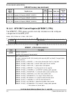


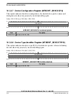


MTBDWT_FCT0 field descriptions (continued)
Field
Description
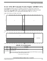
23–20
Reserved
This field is reserved.
This read-only field is reserved and always has the value 0.
19–16
Reserved
This field is reserved.
This read-only field is reserved and always has the value 0.
15–12
DATAVADDR0
Data Value Address 0
Since the MTB_DWT implements two comparators, the DATAVADDR0 field is restricted to values {0,1}.
When the DATAVMATCH bit is asserted, this field defines the comparator number to use for linked
address comparison.
If MTBDWT_COMP0 is used as a data watchpoint and MTBDWT_COMP1 as an address watchpoint,
DATAVADDR0 must be set.
11–10
DATAVSIZE
Data Value Size
For data value matching, this field defines the size of the required data comparison.
00
Byte.
01
Halfword.
10
Word.
11
Reserved. Any attempts to use this value results in UNPREDICTABLE behavior.
9
Reserved
This field is reserved.
This read-only field is reserved and always has the value 0.
8
DATAVMATCH
Data Value Match
When this field is 1, it enables data value comparison. For this implementation, MTBDWT_COMP0
supports address or data value comparisons; MTBDWT_COMP1 only supports address comparisons.
0
Perform address comparison.
1
Perform data value comparison.
7–4
Reserved
This field is reserved.
This read-only field is reserved and always has the value 0.
FUNCTION
Function
Selects the action taken on a comparator match. If MTBDWT_COMP0 is used for a data value and
MTBDWT_COMP1 for an address value, then MTBDWT_FCT1[FUNCTION] must be set to zero. For this
configuration, MTBDWT_MASK1 can be set to a non-zero value, so the combined comparators match on
a range of addresses.
0000
Disabled.
0100
Instruction fetch.
0101
Data operand read.
0110
Data operand write.
0111
Data operand (read + write).
others Reserved. Any attempts to use this value results in UNPREDICTABLE behavior.
Memory map and register definition
KL02 Sub-Family Reference Manual, Rev. 2.1, July 2013
246
Freescale Semiconductor, Inc.
Содержание KKL02Z32CAF4R
Страница 2: ...KL02 Sub Family Reference Manual Rev 2 1 July 2013 2 Freescale Semiconductor Inc...
Страница 24: ...KL02 Sub Family Reference Manual Rev 2 1 July 2013 24 Freescale Semiconductor Inc...
Страница 36: ...Orderable part numbers KL02 Sub Family Reference Manual Rev 2 1 July 2013 36 Freescale Semiconductor Inc...
Страница 76: ...Human machine interfaces HMI KL02 Sub Family Reference Manual Rev 2 1 July 2013 76 Freescale Semiconductor Inc...
Страница 94: ...Module clocks KL02 Sub Family Reference Manual Rev 2 1 July 2013 94 Freescale Semiconductor Inc...
Страница 142: ...Functional description KL02 Sub Family Reference Manual Rev 2 1 July 2013 142 Freescale Semiconductor Inc...
Страница 188: ...Memory map and register descriptions KL02 Sub Family Reference Manual Rev 2 1 July 2013 188 Freescale Semiconductor Inc...
Страница 214: ...Application information KL02 Sub Family Reference Manual Rev 2 1 July 2013 214 Freescale Semiconductor Inc...
Страница 222: ...Memory map register descriptions KL02 Sub Family Reference Manual Rev 2 1 July 2013 222 Freescale Semiconductor Inc...
Страница 256: ...Memory map and register definition KL02 Sub Family Reference Manual Rev 2 1 July 2013 256 Freescale Semiconductor Inc...
Страница 300: ...Functional description KL02 Sub Family Reference Manual Rev 2 1 July 2013 300 Freescale Semiconductor Inc...
Страница 532: ...Functional description KL02 Sub Family Reference Manual Rev 2 1 July 2013 532 Freescale Semiconductor Inc...
Страница 534: ...KL02 Sub Family Reference Manual Rev 2 1 July 2013 534 Freescale Semiconductor Inc...


