


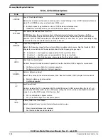


Table 21-11. MCG modes of operation (continued)
Mode
Description
• 0 is written to C1[IREFS]
• C1[FRDIV] must be written to divide external reference clock to be within the range of 31.25
kHz to 39.0625 kHz
In FEE mode, MCGOUTCLK is derived from the FLL clock (DCOCLK) that is controlled by the
external reference clock. The FLL loop will lock the DCO frequency to the FLL factor, as selected by
C4[DRST_DRS] and C4[DMX32] bits, times the external reference frequency, as specified by
C1[FRDIV] and C2[RANGE]. See the C4[DMX32] bit description for more details.
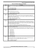
FLL Bypassed Internal
(FBI)
FLL bypassed internal (FBI) mode is entered when all the following conditions occur:
• 01 is written to C1[CLKS]
• 1 is written to C1[IREFS]
• 0 is written to C2[LP]
In FBI mode, the MCGOUTCLK is derived either from the slow (32 kHz IRC) or fast (4 MHz IRC)
internal reference clock, as selected by the C2[IRCS] bit. The FLL is operational but its output is not
used. This mode is useful to allow the FLL to acquire its target frequency while the MCGOUTCLK is
driven from the C2[IRCS] selected internal reference clock. The FLL clock (DCOCLK) is controlled
by the slow internal reference clock, and the DCO clock frequency locks to a multiplication factor, as
selected by C4[DRST_DRS] and C4[DMX32] bits, times the internal reference frequency. See the
C4[DMX32] bit description for more details.
FLL Bypassed External
(FBE)
FLL bypassed external (FBE) mode is entered when all the following conditions occur:
• 10 is written to C1[CLKS]
• 0 is written to C1[IREFS]
• C1[FRDIV] must be written to divide external reference clock to be within the range of 31.25
kHz to 39.0625 kHz.
• 0 is written to C2[LP]
In FBE mode, the MCGOUTCLK is derived from the external reference clock. The FLL is
operational but its output is not used. This mode is useful to allow the FLL to acquire its target
frequency while the MCGOUTCLK is driven from the external reference clock. The FLL clock
(DCOCLK) is controlled by the external reference clock, and the DCO clock frequency locks to a
multiplication factor, as selected by C4[DRST_DRS] and C4[DMX32] bits, times the divided external
reference frequency. See the C4[DMX32] bit description for more details.
Bypassed Low Power
Internal (BLPI)
Bypassed Low Power Internal (BLPI) mode is entered when all the following conditions occur:
• 01 is written to C1[CLKS]
• 1 is written to C1[IREFS]
• 1 is written to C2[LP]
In BLPI mode, MCGOUTCLK is derived from the internal reference clock. The FLL is disabled
Bypassed Low Power
External (BLPE)
Bypassed Low Power External (BLPE) mode is entered when all the following conditions occur:
• 10 is written to C1[CLKS]
• 0 is written to C1[IREFS]
• 1 is written to C2[LP]
In BLPE mode, MCGOUTCLK is derived from the external reference clock. The FLL is disabled
Table continues on the next page...
Functional Description
KL02 Sub-Family Reference Manual, Rev. 2.1, July 2013
276
Freescale Semiconductor, Inc.
Содержание KKL02Z32CAF4R
Страница 2: ...KL02 Sub Family Reference Manual Rev 2 1 July 2013 2 Freescale Semiconductor Inc...
Страница 24: ...KL02 Sub Family Reference Manual Rev 2 1 July 2013 24 Freescale Semiconductor Inc...
Страница 36: ...Orderable part numbers KL02 Sub Family Reference Manual Rev 2 1 July 2013 36 Freescale Semiconductor Inc...
Страница 76: ...Human machine interfaces HMI KL02 Sub Family Reference Manual Rev 2 1 July 2013 76 Freescale Semiconductor Inc...
Страница 94: ...Module clocks KL02 Sub Family Reference Manual Rev 2 1 July 2013 94 Freescale Semiconductor Inc...
Страница 142: ...Functional description KL02 Sub Family Reference Manual Rev 2 1 July 2013 142 Freescale Semiconductor Inc...
Страница 188: ...Memory map and register descriptions KL02 Sub Family Reference Manual Rev 2 1 July 2013 188 Freescale Semiconductor Inc...
Страница 214: ...Application information KL02 Sub Family Reference Manual Rev 2 1 July 2013 214 Freescale Semiconductor Inc...
Страница 222: ...Memory map register descriptions KL02 Sub Family Reference Manual Rev 2 1 July 2013 222 Freescale Semiconductor Inc...
Страница 256: ...Memory map and register definition KL02 Sub Family Reference Manual Rev 2 1 July 2013 256 Freescale Semiconductor Inc...
Страница 300: ...Functional description KL02 Sub Family Reference Manual Rev 2 1 July 2013 300 Freescale Semiconductor Inc...
Страница 532: ...Functional description KL02 Sub Family Reference Manual Rev 2 1 July 2013 532 Freescale Semiconductor Inc...
Страница 534: ...KL02 Sub Family Reference Manual Rev 2 1 July 2013 534 Freescale Semiconductor Inc...


