


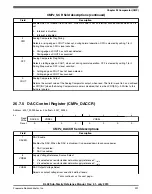


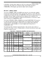


CMPx_DACCR field descriptions (continued)
Field
Description
DACO = (V
in
/64) * (VOSEL[5:0] + 1)
, so the DACO range is from V
in
/64 to V
in
.
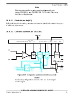
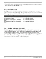
26.7.6 MUX Control Register (CMPx_MUXCR)
Address: 4007_3000h base + 5h offset = 4007_3005h
Bit
7
6
5
4
3
2
1
0
Read
Write
Reset
0
0
0
0
0
0
0
0
CMPx_MUXCR field descriptions
Field
Description
7
Reserved
Bit can be programmed to zero only .
This field is reserved.
6
Reserved
This field is reserved.
This read-only field is reserved and always has the value 0.
5–3
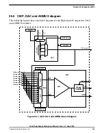
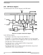
PSEL
Plus Input Mux Control
Determines which input is selected for the plus input of the comparator. For INx inputs, see CMP, DAC,
and ANMUX block diagrams.
NOTE: When an inappropriate operation selects the same input for both muxes, the comparator
automatically shuts down to prevent itself from becoming a noise generator.
000
IN0
001
IN1
010
IN2
011
IN3
100
IN4
101
IN5
110
IN6
111
IN7
MSEL
Minus Input Mux Control
Determines which input is selected for the minus input of the comparator. For INx inputs, see CMP, DAC,
and ANMUX block diagrams.
NOTE: When an inappropriate operation selects the same input for both muxes, the comparator
automatically shuts down to prevent itself from becoming a noise generator.
000
IN0
001
IN1
010
IN2
011
IN3
100
IN4
101
IN5
Table continues on the next page...
Memory map/register definitions
KL02 Sub-Family Reference Manual, Rev. 2.1, July 2013
392
Freescale Semiconductor, Inc.
Содержание KKL02Z32CAF4R
Страница 2: ...KL02 Sub Family Reference Manual Rev 2 1 July 2013 2 Freescale Semiconductor Inc...
Страница 24: ...KL02 Sub Family Reference Manual Rev 2 1 July 2013 24 Freescale Semiconductor Inc...
Страница 36: ...Orderable part numbers KL02 Sub Family Reference Manual Rev 2 1 July 2013 36 Freescale Semiconductor Inc...
Страница 76: ...Human machine interfaces HMI KL02 Sub Family Reference Manual Rev 2 1 July 2013 76 Freescale Semiconductor Inc...
Страница 94: ...Module clocks KL02 Sub Family Reference Manual Rev 2 1 July 2013 94 Freescale Semiconductor Inc...
Страница 142: ...Functional description KL02 Sub Family Reference Manual Rev 2 1 July 2013 142 Freescale Semiconductor Inc...
Страница 188: ...Memory map and register descriptions KL02 Sub Family Reference Manual Rev 2 1 July 2013 188 Freescale Semiconductor Inc...
Страница 214: ...Application information KL02 Sub Family Reference Manual Rev 2 1 July 2013 214 Freescale Semiconductor Inc...
Страница 222: ...Memory map register descriptions KL02 Sub Family Reference Manual Rev 2 1 July 2013 222 Freescale Semiconductor Inc...
Страница 256: ...Memory map and register definition KL02 Sub Family Reference Manual Rev 2 1 July 2013 256 Freescale Semiconductor Inc...
Страница 300: ...Functional description KL02 Sub Family Reference Manual Rev 2 1 July 2013 300 Freescale Semiconductor Inc...
Страница 532: ...Functional description KL02 Sub Family Reference Manual Rev 2 1 July 2013 532 Freescale Semiconductor Inc...
Страница 534: ...KL02 Sub Family Reference Manual Rev 2 1 July 2013 534 Freescale Semiconductor Inc...


