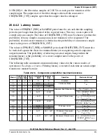


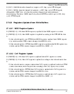
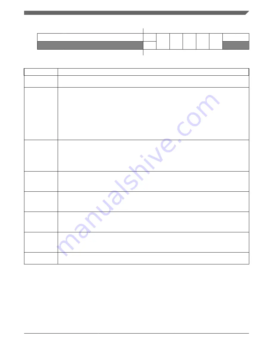
Bit
15
14
13
12
11
10
9
8
7
6
5
4
3
2
1
0
R
W
Reset
0
0
0
0
0
0
0
0
0
0
0
0
0
0
0
0
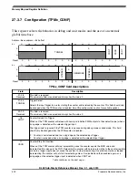
TPMx_CnSC field descriptions
Field
Description
31–8
Reserved
This field is reserved.
This read-only field is reserved and always has the value 0.
7
CHF
Channel Flag
Set by hardware when an event occurs on the channel. CHF is cleared by writing a 1 to the CHF bit.
Writing a 0 to CHF has no effect.
If another event occurs between the CHF sets and the write operation, the write operation has no effect;
therefore, CHF remains set indicating another event has occurred. In this case a CHF interrupt request is
not lost due to the delay in clearing the previous CHF.
0
No channel event has occurred.
1
A channel event has occurred.
6
CHIE
Channel Interrupt Enable
Enables channel interrupts.
0
Disable channel interrupts.
1
Enable channel interrupts.
5
MSB
Channel Mode Select
Used for further selections in the channel logic. Its functionality is dependent on the channel mode. When
a channel is disabled, this bit will not change state until acknowledged in the TPM counter clock domain.
4
MSA
Channel Mode Select
Used for further selections in the channel logic. Its functionality is dependent on the channel mode. When
a channel is disabled, this bit will not change state until acknowledged in the TPM counter clock domain.
3
ELSB
Edge or Level Select
The functionality of ELSB and ELSA depends on the channel mode. When a channel is disabled, this bit
will not change state until acknowledged in the TPM counter clock domain.
2
ELSA
Edge or Level Select
The functionality of ELSB and ELSA depends on the channel mode. When a channel is disabled, this bit
will not change state until acknowledged in the TPM counter clock domain.
Reserved
This field is reserved.
This read-only field is reserved and always has the value 0.
27.3.5 Channel (n) Value (TPMx_CnV)
These registers contain the captured TPM counter value for the input modes or the match
value for the output modes.
In input capture mode, any write to a CnV register is ignored.
Chapter 27 Timer/PWM Module (TPM)
KL02 Sub-Family Reference Manual, Rev. 2.1, July 2013
Freescale Semiconductor, Inc.
417
Содержание KKL02Z32CAF4R
Страница 2: ...KL02 Sub Family Reference Manual Rev 2 1 July 2013 2 Freescale Semiconductor Inc...
Страница 24: ...KL02 Sub Family Reference Manual Rev 2 1 July 2013 24 Freescale Semiconductor Inc...
Страница 36: ...Orderable part numbers KL02 Sub Family Reference Manual Rev 2 1 July 2013 36 Freescale Semiconductor Inc...
Страница 76: ...Human machine interfaces HMI KL02 Sub Family Reference Manual Rev 2 1 July 2013 76 Freescale Semiconductor Inc...
Страница 94: ...Module clocks KL02 Sub Family Reference Manual Rev 2 1 July 2013 94 Freescale Semiconductor Inc...
Страница 142: ...Functional description KL02 Sub Family Reference Manual Rev 2 1 July 2013 142 Freescale Semiconductor Inc...
Страница 188: ...Memory map and register descriptions KL02 Sub Family Reference Manual Rev 2 1 July 2013 188 Freescale Semiconductor Inc...
Страница 214: ...Application information KL02 Sub Family Reference Manual Rev 2 1 July 2013 214 Freescale Semiconductor Inc...
Страница 222: ...Memory map register descriptions KL02 Sub Family Reference Manual Rev 2 1 July 2013 222 Freescale Semiconductor Inc...
Страница 256: ...Memory map and register definition KL02 Sub Family Reference Manual Rev 2 1 July 2013 256 Freescale Semiconductor Inc...
Страница 300: ...Functional description KL02 Sub Family Reference Manual Rev 2 1 July 2013 300 Freescale Semiconductor Inc...
Страница 532: ...Functional description KL02 Sub Family Reference Manual Rev 2 1 July 2013 532 Freescale Semiconductor Inc...
Страница 534: ...KL02 Sub Family Reference Manual Rev 2 1 July 2013 534 Freescale Semiconductor Inc...


