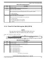
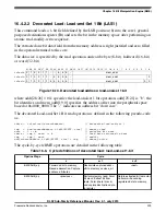

1
2
3
4
next
5..v_wxyz
next
next
400v_wxyz
next
next
5..v_wxyz
rdata
next
rdata
ubfx
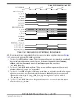
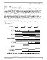
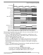
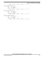
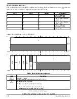
CYCLE RULER
hclk
BME AHB Input Bus
mx_haddr
mx_hattr
mx_hwrite
mx_hwdata
mx_hrdata
mx_hready
BME AHB Output Bus
sx_haddr
sx_hattr
sx_hwrite
sx_hwdata
sx_hrdata
sx_hready
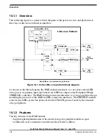
BME Datapath
control_state_dp1
control_state_dp2
reg_addr_data_dp
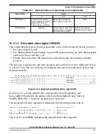
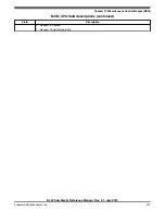
Figure 16-8. Decorated load: unsigned bit field insert timing diagram
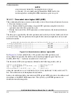
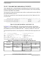
The decorated unsigned bit field extract follows the same execution template shown in
the above figure, a 2-cycle read operation:
• Cycle x, 1st AHB address phase: Read from input bus is translated into a read
operation on the output bus with the actual memory address (with the decoration
removed) and then captured in a register
• Cycle x+1, 2nd AHB address phase: Idle cycle
• Cycle x+1, 1st AHB data phase: A bit mask is generated based on the starting bit
position and the field width; the mask is AND'ed with the memory read data to
isolate the bit field; the resulting data is captured in a data register; the input bus
cycle is stalled
• Cycle x+2, 2nd AHB data phase: Registered data is logically right-aligned for proper
alignment and driven onto the input read data bus
NOTE
Any wait states inserted by the peripheral slave device
(sx_hready = 0) are simply passed through the BME back to the
master input bus, stalling the AHB transaction cycle for cycle.
Chapter 16 Bit Manipulation Engine (BME)
KL02 Sub-Family Reference Manual, Rev. 2.1, July 2013
Freescale Semiconductor, Inc.
207
Содержание KKL02Z32CAF4R
Страница 2: ...KL02 Sub Family Reference Manual Rev 2 1 July 2013 2 Freescale Semiconductor Inc...
Страница 24: ...KL02 Sub Family Reference Manual Rev 2 1 July 2013 24 Freescale Semiconductor Inc...
Страница 36: ...Orderable part numbers KL02 Sub Family Reference Manual Rev 2 1 July 2013 36 Freescale Semiconductor Inc...
Страница 76: ...Human machine interfaces HMI KL02 Sub Family Reference Manual Rev 2 1 July 2013 76 Freescale Semiconductor Inc...
Страница 94: ...Module clocks KL02 Sub Family Reference Manual Rev 2 1 July 2013 94 Freescale Semiconductor Inc...
Страница 142: ...Functional description KL02 Sub Family Reference Manual Rev 2 1 July 2013 142 Freescale Semiconductor Inc...
Страница 188: ...Memory map and register descriptions KL02 Sub Family Reference Manual Rev 2 1 July 2013 188 Freescale Semiconductor Inc...
Страница 214: ...Application information KL02 Sub Family Reference Manual Rev 2 1 July 2013 214 Freescale Semiconductor Inc...
Страница 222: ...Memory map register descriptions KL02 Sub Family Reference Manual Rev 2 1 July 2013 222 Freescale Semiconductor Inc...
Страница 256: ...Memory map and register definition KL02 Sub Family Reference Manual Rev 2 1 July 2013 256 Freescale Semiconductor Inc...
Страница 300: ...Functional description KL02 Sub Family Reference Manual Rev 2 1 July 2013 300 Freescale Semiconductor Inc...
Страница 532: ...Functional description KL02 Sub Family Reference Manual Rev 2 1 July 2013 532 Freescale Semiconductor Inc...
Страница 534: ...KL02 Sub Family Reference Manual Rev 2 1 July 2013 534 Freescale Semiconductor Inc...


