


No two slaves in the system can have the same address. If the I2C module is the master, it
must not transmit an address that is equal to its own slave address. The I2C module
cannot be master and slave at the same time. However, if arbitration is lost during an
address cycle, the I2C module reverts to slave mode and operates correctly even if it is
being addressed by another master.
30.4.1.3 Data transfers
When successful slave addressing is achieved, data transfer can proceed on a byte-by-
byte basis in the direction specified by the R/W bit sent by the calling master.
All transfers that follow an address cycle are referred to as data transfers, even if they
carry subaddress information for the slave device.
Each data byte is 8 bits long. Data may be changed only while SCL is low. Data must be
held stable while SCL is high. There is one clock pulse on SCL for each data bit, and the
MSB is transferred first. Each data byte is followed by a ninth (acknowledge) bit, which
is signaled from the receiving device by pulling SDA low at the ninth clock. In summary,
one complete data transfer needs nine clock pulses.
If the slave receiver does not acknowledge the master in the ninth bit, the slave must
leave SDA high. The master interprets the failed acknowledgement as an unsuccessful
data transfer.
If the master receiver does not acknowledge the slave transmitter after a data byte
transmission, the slave interprets it as an end to data transfer and releases the SDA line.
In the case of a failed acknowledgement by either the slave or master, the data transfer is
aborted and the master does one of two things:
• Relinquishes the bus by generating a STOP signal.
• Commences a new call by generating a repeated START signal.
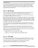
30.4.1.4 STOP signal
The master can terminate the communication by generating a STOP signal to free the
bus. A STOP signal is defined as a low-to-high transition of SDA while SCL is asserted.
The master can generate a STOP signal even if the slave has generated an
acknowledgement, at which point the slave must release the bus.
Functional description
KL02 Sub-Family Reference Manual, Rev. 2.1, July 2013
484
Freescale Semiconductor, Inc.
Содержание KKL02Z32CAF4R
Страница 2: ...KL02 Sub Family Reference Manual Rev 2 1 July 2013 2 Freescale Semiconductor Inc...
Страница 24: ...KL02 Sub Family Reference Manual Rev 2 1 July 2013 24 Freescale Semiconductor Inc...
Страница 36: ...Orderable part numbers KL02 Sub Family Reference Manual Rev 2 1 July 2013 36 Freescale Semiconductor Inc...
Страница 76: ...Human machine interfaces HMI KL02 Sub Family Reference Manual Rev 2 1 July 2013 76 Freescale Semiconductor Inc...
Страница 94: ...Module clocks KL02 Sub Family Reference Manual Rev 2 1 July 2013 94 Freescale Semiconductor Inc...
Страница 142: ...Functional description KL02 Sub Family Reference Manual Rev 2 1 July 2013 142 Freescale Semiconductor Inc...
Страница 188: ...Memory map and register descriptions KL02 Sub Family Reference Manual Rev 2 1 July 2013 188 Freescale Semiconductor Inc...
Страница 214: ...Application information KL02 Sub Family Reference Manual Rev 2 1 July 2013 214 Freescale Semiconductor Inc...
Страница 222: ...Memory map register descriptions KL02 Sub Family Reference Manual Rev 2 1 July 2013 222 Freescale Semiconductor Inc...
Страница 256: ...Memory map and register definition KL02 Sub Family Reference Manual Rev 2 1 July 2013 256 Freescale Semiconductor Inc...
Страница 300: ...Functional description KL02 Sub Family Reference Manual Rev 2 1 July 2013 300 Freescale Semiconductor Inc...
Страница 532: ...Functional description KL02 Sub Family Reference Manual Rev 2 1 July 2013 532 Freescale Semiconductor Inc...
Страница 534: ...KL02 Sub Family Reference Manual Rev 2 1 July 2013 534 Freescale Semiconductor Inc...


