

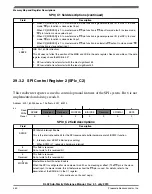


If C1[CPHA] is set, even numbered edges on the SPSCK input cause the data at the serial
data input pin to be latched. Odd numbered edges cause the value previously latched
from the serial data input pin to shift into the LSB or MSB of the SPI shift register,
depending on C1[LSBFE].
When C1[CPHA] is set, the first edge is used to get the first data bit onto the serial data
output pin. When C1[CPHA] is clear and the SS input is low (slave selected), the first bit
of the SPI data is driven out of the serial data output pin. After the eighth shift, the
transfer is considered complete and the received data is transferred into the SPI Data
register. To indicate transfer is complete, the SPRF flag in the SPI Status Register is set.
Note
A change of the bits C2[BIDIROE] with C2[SPC0] set,
C1[CPOL], C1[CPHA], C1[SSOE], C1[LSBFE],
C2[MODFEN], and C2[SPC0] in slave mode will corrupt a
transmission in progress and must be avoided.
29.4.4 SPI clock formats
To accommodate a wide variety of synchronous serial peripherals from different
manufacturers, the SPI system has a Clock Polarity (CPOL) bit and a Clock Phase
(CPHA) control bit in the Control Register 1 to select one of four clock formats for data
transfers. C1[CPOL] selectively inserts an inverter in series with the clock. C1[CPHA]
chooses between two different clock phase relationships between the clock and data.
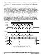
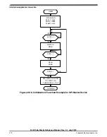
The following figure shows the clock formats when CPHA = 1. At the top of the figure,
the eight bit times are shown for reference with bit 1 starting at the first SPSCK edge and
bit 8 ending one-half SPSCK cycle after the eighth SPSCK edge. The MSB first and LSB
first lines show the order of SPI data bits depending on the setting in LSBFE. Both
variations of SPSCK polarity are shown, but only one of these waveforms applies for a
specific transfer, depending on the value in C1[CPOL]. The SAMPLE IN waveform
applies to the MOSI input of a slave or the MISO input of a master. The MOSI waveform
applies to the MOSI output pin from a master and the MISO waveform applies to the
MISO output from a slave. The SS OUT waveform applies to the slave select output from
a master (provided C2[MODFEN] and C1[SSOE] = 1). The master SS output goes to
active low one-half SPSCK cycle before the start of the transfer and goes back high at the
end of the eighth bit time of the transfer. The SS IN waveform applies to the slave select
input of a slave.
Functional description
KL02 Sub-Family Reference Manual, Rev. 2.1, July 2013
458
Freescale Semiconductor, Inc.
Содержание KKL02Z32CAF4R
Страница 2: ...KL02 Sub Family Reference Manual Rev 2 1 July 2013 2 Freescale Semiconductor Inc...
Страница 24: ...KL02 Sub Family Reference Manual Rev 2 1 July 2013 24 Freescale Semiconductor Inc...
Страница 36: ...Orderable part numbers KL02 Sub Family Reference Manual Rev 2 1 July 2013 36 Freescale Semiconductor Inc...
Страница 76: ...Human machine interfaces HMI KL02 Sub Family Reference Manual Rev 2 1 July 2013 76 Freescale Semiconductor Inc...
Страница 94: ...Module clocks KL02 Sub Family Reference Manual Rev 2 1 July 2013 94 Freescale Semiconductor Inc...
Страница 142: ...Functional description KL02 Sub Family Reference Manual Rev 2 1 July 2013 142 Freescale Semiconductor Inc...
Страница 188: ...Memory map and register descriptions KL02 Sub Family Reference Manual Rev 2 1 July 2013 188 Freescale Semiconductor Inc...
Страница 214: ...Application information KL02 Sub Family Reference Manual Rev 2 1 July 2013 214 Freescale Semiconductor Inc...
Страница 222: ...Memory map register descriptions KL02 Sub Family Reference Manual Rev 2 1 July 2013 222 Freescale Semiconductor Inc...
Страница 256: ...Memory map and register definition KL02 Sub Family Reference Manual Rev 2 1 July 2013 256 Freescale Semiconductor Inc...
Страница 300: ...Functional description KL02 Sub Family Reference Manual Rev 2 1 July 2013 300 Freescale Semiconductor Inc...
Страница 532: ...Functional description KL02 Sub Family Reference Manual Rev 2 1 July 2013 532 Freescale Semiconductor Inc...
Страница 534: ...KL02 Sub Family Reference Manual Rev 2 1 July 2013 534 Freescale Semiconductor Inc...


