


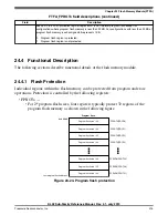


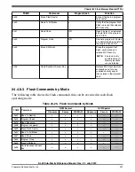
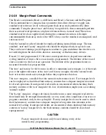


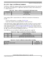


24.4.8 Flash Command Operations
Flash command operations are typically used to modify flash memory contents. The next
sections describe:
• The command write sequence used to set flash command parameters and launch
execution
• A description of all flash commands available
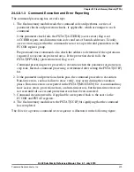
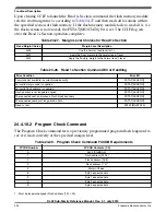
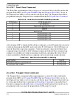
24.4.8.1 Command Write Sequence
Flash commands are specified using a command write sequence illustrated in
. The flash memory module performs various checks on the command (FCCOB)
content and continues with command execution if all requirements are fulfilled.
Before launching a command, the ACCERR and FPVIOL bits in the FSTAT register
must be zero and the CCIF flag must read 1 to verify that any previous command has
completed. If CCIF is zero, the previous command execution is still active, a new
command write sequence cannot be started, and all writes to the FCCOB registers are
ignored.
Attempts to launch a flash command in VLP mode will be ignored.
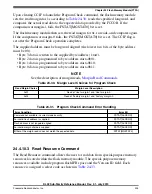
24.4.8.1.1 Load the FCCOB Registers
The user must load the FCCOB registers with all parameters required by the desired flash
command. The individual registers that make up the FCCOB data set can be written in
any order.
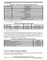
24.4.8.1.2 Launch the Command by Clearing CCIF
Once all relevant command parameters have been loaded, the user launches the command
by clearing the FSTAT[CCIF] bit by writing a '1' to it. The CCIF flag remains zero until
the flash command completes.
The FSTAT register contains a blocking mechanism that prevents a new command from
launching (can't clear CCIF) if the previous command resulted in an access error
(FSTAT[ACCERR]=1) or a protection violation (FSTAT[FPVIOL]=1). In error
scenarios, two writes to FSTAT are required to initiate the next command: the first write
clears the error flags, the second write clears CCIF.
Functional Description
KL02 Sub-Family Reference Manual, Rev. 2.1, July 2013
318
Freescale Semiconductor, Inc.
Содержание KKL02Z32CAF4R
Страница 2: ...KL02 Sub Family Reference Manual Rev 2 1 July 2013 2 Freescale Semiconductor Inc...
Страница 24: ...KL02 Sub Family Reference Manual Rev 2 1 July 2013 24 Freescale Semiconductor Inc...
Страница 36: ...Orderable part numbers KL02 Sub Family Reference Manual Rev 2 1 July 2013 36 Freescale Semiconductor Inc...
Страница 76: ...Human machine interfaces HMI KL02 Sub Family Reference Manual Rev 2 1 July 2013 76 Freescale Semiconductor Inc...
Страница 94: ...Module clocks KL02 Sub Family Reference Manual Rev 2 1 July 2013 94 Freescale Semiconductor Inc...
Страница 142: ...Functional description KL02 Sub Family Reference Manual Rev 2 1 July 2013 142 Freescale Semiconductor Inc...
Страница 188: ...Memory map and register descriptions KL02 Sub Family Reference Manual Rev 2 1 July 2013 188 Freescale Semiconductor Inc...
Страница 214: ...Application information KL02 Sub Family Reference Manual Rev 2 1 July 2013 214 Freescale Semiconductor Inc...
Страница 222: ...Memory map register descriptions KL02 Sub Family Reference Manual Rev 2 1 July 2013 222 Freescale Semiconductor Inc...
Страница 256: ...Memory map and register definition KL02 Sub Family Reference Manual Rev 2 1 July 2013 256 Freescale Semiconductor Inc...
Страница 300: ...Functional description KL02 Sub Family Reference Manual Rev 2 1 July 2013 300 Freescale Semiconductor Inc...
Страница 532: ...Functional description KL02 Sub Family Reference Manual Rev 2 1 July 2013 532 Freescale Semiconductor Inc...
Страница 534: ...KL02 Sub Family Reference Manual Rev 2 1 July 2013 534 Freescale Semiconductor Inc...


