
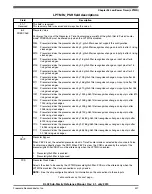


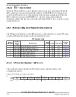


SPI0_C1 field descriptions (continued)
Field
Description
0
When C2[MODFEN] is 0: In master mode, SS pin function is general-purpose I/O (not SPI). In slave
mode, SS pin function is slave select input.
When C2[MODFEN] is 1: In master mode, SS pin function is SS input for mode fault. In slave mode,
SS pin function is slave select input.
1
When C2[MODFEN] is 0: In master mode, SS pin function is general-purpose I/O (not SPI). In slave
mode, SS pin function is slave select input.
When C2[MODFEN] is 1: In master mode, SS pin function is automatic SS output. In slave mode: SS
pin function is slave select input.
0
LSBFE
LSB First (shifter direction)
This bit does not affect the position of the MSB and LSB in the data register. Reads and writes of the data
register always have the MSB in bit 7.
0
SPI serial data transfers start with the most significant bit.
1
SPI serial data transfers start with the least significant bit.
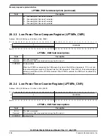
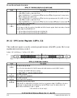
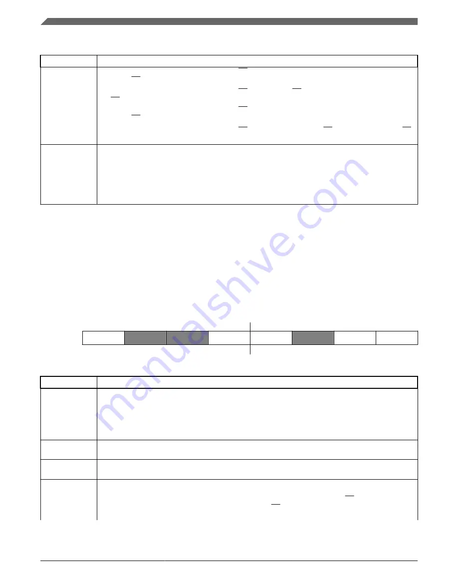
29.3.2 SPI Control Register 2 (SPIx_C2)
This read/write register is used to control optional features of the SPI system. Bit 6 is not
implemented and always reads 0.
Address: 4007_6000h base + 1h offset = 4007_6001h
Bit
7
6
5
4
3
2
1
0
Read
Write
Reset
0
0
0
0
0
0
0
0
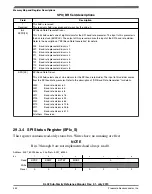
SPI0_C2 field descriptions
Field
Description
7
SPMIE
SPI Match Interrupt Enable
This is the interrupt enable bit for the SPI receive data buffer hardware match (SPMF) function.
0
Interrupts from SPMF inhibited (use polling)
1
When SPMF is 1, requests a hardware interrupt
6
Reserved
This field is reserved.
Do not write to this reserved bit.
5
Reserved
This field is reserved.
Do not write to this reserved bit.
4
MODFEN
Master Mode-Fault Function Enable
When the SPI is configured for slave mode, this bit has no meaning or effect. (The SS pin is the slave
select input.) In master mode, this bit determines how the SS pin is used. For details, refer to the
description of the SSOE bit in the C1 register.
Table continues on the next page...
Memory Map and Register Descriptions
KL02 Sub-Family Reference Manual, Rev. 2.1, July 2013
450
Freescale Semiconductor, Inc.
Содержание KKL02Z32CAF4R
Страница 2: ...KL02 Sub Family Reference Manual Rev 2 1 July 2013 2 Freescale Semiconductor Inc...
Страница 24: ...KL02 Sub Family Reference Manual Rev 2 1 July 2013 24 Freescale Semiconductor Inc...
Страница 36: ...Orderable part numbers KL02 Sub Family Reference Manual Rev 2 1 July 2013 36 Freescale Semiconductor Inc...
Страница 76: ...Human machine interfaces HMI KL02 Sub Family Reference Manual Rev 2 1 July 2013 76 Freescale Semiconductor Inc...
Страница 94: ...Module clocks KL02 Sub Family Reference Manual Rev 2 1 July 2013 94 Freescale Semiconductor Inc...
Страница 142: ...Functional description KL02 Sub Family Reference Manual Rev 2 1 July 2013 142 Freescale Semiconductor Inc...
Страница 188: ...Memory map and register descriptions KL02 Sub Family Reference Manual Rev 2 1 July 2013 188 Freescale Semiconductor Inc...
Страница 214: ...Application information KL02 Sub Family Reference Manual Rev 2 1 July 2013 214 Freescale Semiconductor Inc...
Страница 222: ...Memory map register descriptions KL02 Sub Family Reference Manual Rev 2 1 July 2013 222 Freescale Semiconductor Inc...
Страница 256: ...Memory map and register definition KL02 Sub Family Reference Manual Rev 2 1 July 2013 256 Freescale Semiconductor Inc...
Страница 300: ...Functional description KL02 Sub Family Reference Manual Rev 2 1 July 2013 300 Freescale Semiconductor Inc...
Страница 532: ...Functional description KL02 Sub Family Reference Manual Rev 2 1 July 2013 532 Freescale Semiconductor Inc...
Страница 534: ...KL02 Sub Family Reference Manual Rev 2 1 July 2013 534 Freescale Semiconductor Inc...


