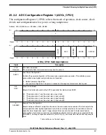
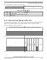
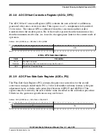
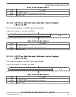
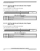
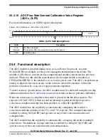


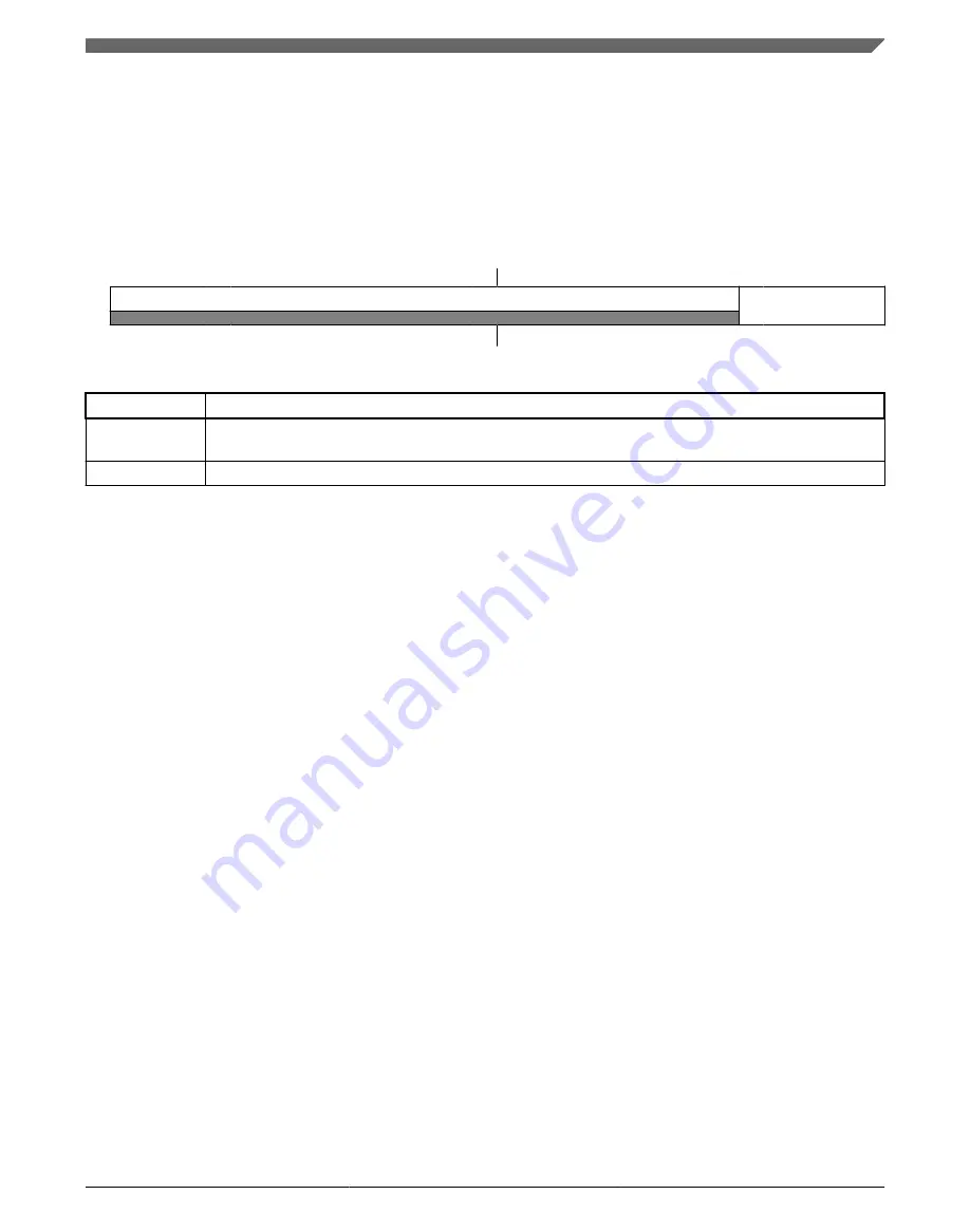
25.3.16 ADC Plus-Side General Calibration Value Register
(ADCx_CLP0)
For more information, see CLPD register description.
Address: 4003_B000h base + 4Ch offset = 4003_B04Ch
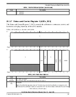
Bit
31 30 29 28 27 26 25 24 23 22 21 20 19 18 17 16 15 14 13 12 11 10
9
8
7
6
5
4
3
2
1
0
R
W
Reset
0 0 0 0 0 0 0 0 0 0 0 0 0 0 0 0 0 0 0 0 0 0 0 0 0 0 1 0 0 0 0 0
ADCx_CLP0 field descriptions
Field
Description
31–6
Reserved
This field is reserved.
This read-only field is reserved and always has the value 0.
CLP0
Calibration Value
25.4 Functional description
The ADC module is disabled during reset, in Low-Power Stop mode, or when
SC1n[ADCH] are all high; see the power management information for details. The
module is idle when a conversion has completed and another conversion has not been
initiated. When it is idle and the asynchronous clock output enable is disabled, or
CFG2[ADACKEN]= 0, the module is in its lowest power state. The ADC can perform an
analog-to-digital conversion on any of the software selectable channels. All modes
perform conversion by a successive approximation algorithm.
To meet accuracy specifications, the ADC module must be calibrated using the on-chip
calibration function. See
for details on how to perform calibration.
When the conversion is completed, the result is placed in the Rn data registers. The
respective SC1n[COCO] is then set and an interrupt is generated if the respective
conversion complete interrupt has been enabled, or, when SC1n[AIEN]=1.
The ADC module has the capability of automatically comparing the result of a
conversion with the contents of the CV1 and CV2 registers. The compare function is
enabled by setting SC2[ACFE] and operates in any of the conversion modes and
configurations.
The ADC module has the capability of automatically averaging the result of multiple
conversions. The hardware average function is enabled by setting SC3[AVGE] and
operates in any of the conversion modes and configurations.
Chapter 25 Analog-to-Digital Converter (ADC)
KL02 Sub-Family Reference Manual, Rev. 2.1, July 2013
Freescale Semiconductor, Inc.
359
Содержание KKL02Z32CAF4R
Страница 2: ...KL02 Sub Family Reference Manual Rev 2 1 July 2013 2 Freescale Semiconductor Inc...
Страница 24: ...KL02 Sub Family Reference Manual Rev 2 1 July 2013 24 Freescale Semiconductor Inc...
Страница 36: ...Orderable part numbers KL02 Sub Family Reference Manual Rev 2 1 July 2013 36 Freescale Semiconductor Inc...
Страница 76: ...Human machine interfaces HMI KL02 Sub Family Reference Manual Rev 2 1 July 2013 76 Freescale Semiconductor Inc...
Страница 94: ...Module clocks KL02 Sub Family Reference Manual Rev 2 1 July 2013 94 Freescale Semiconductor Inc...
Страница 142: ...Functional description KL02 Sub Family Reference Manual Rev 2 1 July 2013 142 Freescale Semiconductor Inc...
Страница 188: ...Memory map and register descriptions KL02 Sub Family Reference Manual Rev 2 1 July 2013 188 Freescale Semiconductor Inc...
Страница 214: ...Application information KL02 Sub Family Reference Manual Rev 2 1 July 2013 214 Freescale Semiconductor Inc...
Страница 222: ...Memory map register descriptions KL02 Sub Family Reference Manual Rev 2 1 July 2013 222 Freescale Semiconductor Inc...
Страница 256: ...Memory map and register definition KL02 Sub Family Reference Manual Rev 2 1 July 2013 256 Freescale Semiconductor Inc...
Страница 300: ...Functional description KL02 Sub Family Reference Manual Rev 2 1 July 2013 300 Freescale Semiconductor Inc...
Страница 532: ...Functional description KL02 Sub Family Reference Manual Rev 2 1 July 2013 532 Freescale Semiconductor Inc...
Страница 534: ...KL02 Sub Family Reference Manual Rev 2 1 July 2013 534 Freescale Semiconductor Inc...


