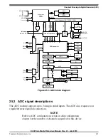
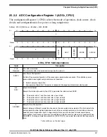
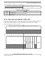
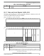
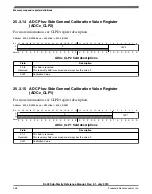


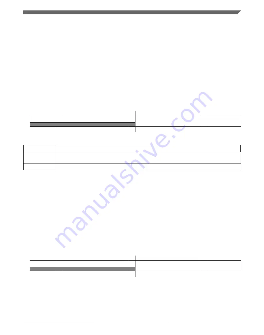
25.3.8 ADC Offset Correction Register (ADCx_OFS)
The ADC Offset Correction Register (OFS) contains the user-selected or calibration-
generated offset error correction value. This register is a 2’s complement, left-justified,
16-bit value . The value in OFS is subtracted from the conversion and the result is
transferred into the result registers, Rn. If the result is greater than the maximum or less
than the minimum result value, it is forced to the appropriate limit for the current mode of
operation.
Address: 4003_B000h base + 28h offset = 4003_B028h
Bit
31 30 29 28 27 26 25 24 23 22 21 20 19 18 17 16 15 14 13 12 11 10
9
8
7
6
5
4
3
2
1
0
R
W
Reset
0 0 0 0 0 0 0 0 0 0 0 0 0 0 0 0 0 0 0 0 0 0 0 0 0 0 0 0 0 1 0 0
ADCx_OFS field descriptions
Field
Description
31–16
Reserved
This field is reserved.
This read-only field is reserved and always has the value 0.
OFS
Offset Error Correction Value
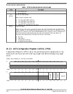
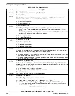
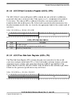
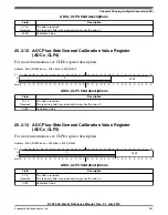
25.3.9 ADC Plus-Side Gain Register (ADCx_PG)
The Plus-Side Gain Register (PG) contains the gain error correction for the overall
conversion in single-ended mode. PG, a 16-bit real number in binary format, is the gain
adjustment factor, with the radix point fixed between ADPG15 and ADPG14. This
register must be written by the user with the value described in the calibration procedure.
Otherwise, the gain error specifications may not be met.
Address: 4003_B000h base + 2Ch offset = 4003_B02Ch
Bit
31 30 29 28 27 26 25 24 23 22 21 20 19 18 17 16 15 14 13 12 11 10
9
8
7
6
5
4
3
2
1
0
R
W
Reset
0 0 0 0 0 0 0 0 0 0 0 0 0 0 0 0 1 0 0 0 0 0 1 0 0 0 0 0 0 0 0 0
Chapter 25 Analog-to-Digital Converter (ADC)
KL02 Sub-Family Reference Manual, Rev. 2.1, July 2013
Freescale Semiconductor, Inc.
355
Содержание KKL02Z32CAF4R
Страница 2: ...KL02 Sub Family Reference Manual Rev 2 1 July 2013 2 Freescale Semiconductor Inc...
Страница 24: ...KL02 Sub Family Reference Manual Rev 2 1 July 2013 24 Freescale Semiconductor Inc...
Страница 36: ...Orderable part numbers KL02 Sub Family Reference Manual Rev 2 1 July 2013 36 Freescale Semiconductor Inc...
Страница 76: ...Human machine interfaces HMI KL02 Sub Family Reference Manual Rev 2 1 July 2013 76 Freescale Semiconductor Inc...
Страница 94: ...Module clocks KL02 Sub Family Reference Manual Rev 2 1 July 2013 94 Freescale Semiconductor Inc...
Страница 142: ...Functional description KL02 Sub Family Reference Manual Rev 2 1 July 2013 142 Freescale Semiconductor Inc...
Страница 188: ...Memory map and register descriptions KL02 Sub Family Reference Manual Rev 2 1 July 2013 188 Freescale Semiconductor Inc...
Страница 214: ...Application information KL02 Sub Family Reference Manual Rev 2 1 July 2013 214 Freescale Semiconductor Inc...
Страница 222: ...Memory map register descriptions KL02 Sub Family Reference Manual Rev 2 1 July 2013 222 Freescale Semiconductor Inc...
Страница 256: ...Memory map and register definition KL02 Sub Family Reference Manual Rev 2 1 July 2013 256 Freescale Semiconductor Inc...
Страница 300: ...Functional description KL02 Sub Family Reference Manual Rev 2 1 July 2013 300 Freescale Semiconductor Inc...
Страница 532: ...Functional description KL02 Sub Family Reference Manual Rev 2 1 July 2013 532 Freescale Semiconductor Inc...
Страница 534: ...KL02 Sub Family Reference Manual Rev 2 1 July 2013 534 Freescale Semiconductor Inc...


