


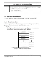


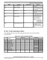


Upon clearing CCIF to launch the Program Check command, the flash memory module
sets the read margin for 1s according to
, reads the specified longword, and
compares the actual read data to the expected data provided by the FCCOB. If the
comparison at margin-1 fails, the FSTAT[MGSTAT0] bit is set.
The flash memory module then sets the read margin for 0s, re-reads, and compares again.
If the comparison at margin-0 fails, the FSTAT[MGSTAT0] bit is set. The CCIF flag is
set after the Program Check operation completes.
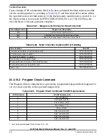
The supplied address must be longword aligned (the lowest two bits of the byte address
must be 00):
• Byte 3 data is written to the supplied byte address ('start'),
• Byte 2 data is programmed to byte address start+0b01,
• Byte 1 data is programmed to byte address start+0b10,
• Byte 0 data is programmed to byte address start+0b11.
NOTE
See the description of margin reads,
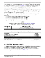
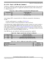
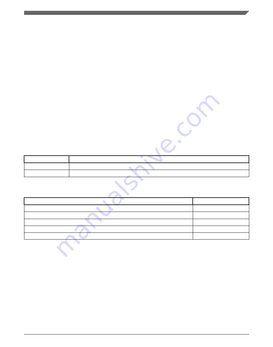
Table 24-30. Margin Level Choices for Program Check
Read Margin Choice
Margin Level Description
0x01
Read at 'User' margin-1 and 'User' margin-0
0x02
Read at 'Factory' margin-1 and 'Factory' margin-0
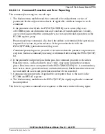
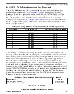
Table 24-31. Program Check Command Error Handling
Error Condition
Error Bit
Command not available in current mode/security
FSTAT[ACCERR]
An invalid flash address is supplied
FSTAT[ACCERR]
Flash address is not longword aligned
FSTAT[ACCERR]
An invalid margin choice is supplied
FSTAT[ACCERR]
Either of the margin reads does not match the expected data
FSTAT[MGSTAT0]
24.4.10.3 Read Resource Command
The Read Resource command allows the user to read data from special-purpose memory
resources located within the flash memory module. The special-purpose memory
resources available include program flash IFR space and the Version ID field. Each
resource is assigned a select code as shown in
.
Chapter 24 Flash Memory Module (FTFA)
KL02 Sub-Family Reference Manual, Rev. 2.1, July 2013
Freescale Semiconductor, Inc.
325
Содержание KKL02Z32CAF4R
Страница 2: ...KL02 Sub Family Reference Manual Rev 2 1 July 2013 2 Freescale Semiconductor Inc...
Страница 24: ...KL02 Sub Family Reference Manual Rev 2 1 July 2013 24 Freescale Semiconductor Inc...
Страница 36: ...Orderable part numbers KL02 Sub Family Reference Manual Rev 2 1 July 2013 36 Freescale Semiconductor Inc...
Страница 76: ...Human machine interfaces HMI KL02 Sub Family Reference Manual Rev 2 1 July 2013 76 Freescale Semiconductor Inc...
Страница 94: ...Module clocks KL02 Sub Family Reference Manual Rev 2 1 July 2013 94 Freescale Semiconductor Inc...
Страница 142: ...Functional description KL02 Sub Family Reference Manual Rev 2 1 July 2013 142 Freescale Semiconductor Inc...
Страница 188: ...Memory map and register descriptions KL02 Sub Family Reference Manual Rev 2 1 July 2013 188 Freescale Semiconductor Inc...
Страница 214: ...Application information KL02 Sub Family Reference Manual Rev 2 1 July 2013 214 Freescale Semiconductor Inc...
Страница 222: ...Memory map register descriptions KL02 Sub Family Reference Manual Rev 2 1 July 2013 222 Freescale Semiconductor Inc...
Страница 256: ...Memory map and register definition KL02 Sub Family Reference Manual Rev 2 1 July 2013 256 Freescale Semiconductor Inc...
Страница 300: ...Functional description KL02 Sub Family Reference Manual Rev 2 1 July 2013 300 Freescale Semiconductor Inc...
Страница 532: ...Functional description KL02 Sub Family Reference Manual Rev 2 1 July 2013 532 Freescale Semiconductor Inc...
Страница 534: ...KL02 Sub Family Reference Manual Rev 2 1 July 2013 534 Freescale Semiconductor Inc...


