

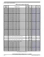


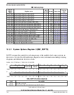

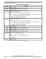


SIM memory map
Absolute
address
(hex)
Register name
Width
(in bits)
Access Reset value
Section/
page
4004_8004 System Options Register 2 (SIM_SOPT2)
32
R/W
0000_0000h
4004_800C System Options Register 4 (SIM_SOPT4)
32
R/W
0000_0000h
4004_8010 System Options Register 5 (SIM_SOPT5)
32
R/W
0000_0000h
4004_8018 System Options Register 7 (SIM_SOPT7)
32
R/W
0000_0000h
4004_8024 System Device Identification Register (SIM_SDID)
32
R
4004_8034 System Clock Gating Control Register 4 (SIM_SCGC4)
32
R/W
E000_0030h
4004_8038 System Clock Gating Control Register 5 (SIM_SCGC5)
32
R/W
0000_0180h
4004_803C System Clock Gating Control Register 6 (SIM_SCGC6)
32
R/W
0000_0001h
4004_8044 System Clock Divider Register 1 (SIM_CLKDIV1)
32
R/W
4004_804C Flash Configuration Register 1 (SIM_FCFG1)
32
R/W
4004_8050 Flash Configuration Register 2 (SIM_FCFG2)
32
R
4004_8058 Unique Identification Register Mid-High (SIM_UIDMH)
32
R
4004_805C Unique Identification Register Mid Low (SIM_UIDML)
32
R
4004_8060 Unique Identification Register Low (SIM_UIDL)
32
R
4004_8100 COP Control Register (SIM_COPC)
32
R/W
0000_000Ch
4004_8104 Service COP Register (SIM_SRVCOP)
32
W
0000_0000h
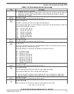
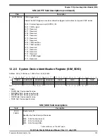
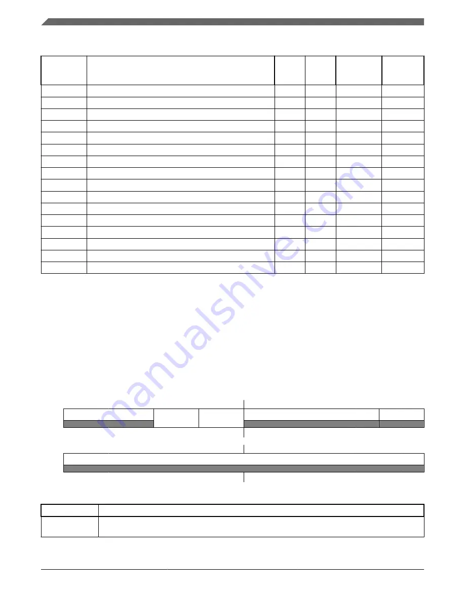
12.2.1 System Options Register 2 (SIM_SOPT2)
SOPT2 contains the controls for selecting many of the module clock source options on
this device. See the Clock Distribution chapter for more information including clocking
diagrams and definitions of device clocks.
Address: 4004_7000h base + 1004h offset = 4004_8004h
Bit
31
30
29
28
27
26
25
24
23
22
21
20
19
18
17
16
R
W
Reset
0
0
0
0
0
0
0
0
0
0
0
0
0
0
0
0
Bit
15
14
13
12
11
10
9
8
7
6
5
4
3
2
1
0
R
W
Reset
0
0
0
0
0
0
0
0
0
0
0
0
0
0
0
0
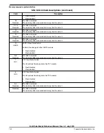
SIM_SOPT2 field descriptions
Field
Description
31–28
Reserved
This field is reserved.
This read-only field is reserved and always has the value 0.
Table continues on the next page...
Memory map and register definition
KL02 Sub-Family Reference Manual, Rev. 2.1, July 2013
144
Freescale Semiconductor, Inc.
Содержание KKL02Z32CAF4R
Страница 2: ...KL02 Sub Family Reference Manual Rev 2 1 July 2013 2 Freescale Semiconductor Inc...
Страница 24: ...KL02 Sub Family Reference Manual Rev 2 1 July 2013 24 Freescale Semiconductor Inc...
Страница 36: ...Orderable part numbers KL02 Sub Family Reference Manual Rev 2 1 July 2013 36 Freescale Semiconductor Inc...
Страница 76: ...Human machine interfaces HMI KL02 Sub Family Reference Manual Rev 2 1 July 2013 76 Freescale Semiconductor Inc...
Страница 94: ...Module clocks KL02 Sub Family Reference Manual Rev 2 1 July 2013 94 Freescale Semiconductor Inc...
Страница 142: ...Functional description KL02 Sub Family Reference Manual Rev 2 1 July 2013 142 Freescale Semiconductor Inc...
Страница 188: ...Memory map and register descriptions KL02 Sub Family Reference Manual Rev 2 1 July 2013 188 Freescale Semiconductor Inc...
Страница 214: ...Application information KL02 Sub Family Reference Manual Rev 2 1 July 2013 214 Freescale Semiconductor Inc...
Страница 222: ...Memory map register descriptions KL02 Sub Family Reference Manual Rev 2 1 July 2013 222 Freescale Semiconductor Inc...
Страница 256: ...Memory map and register definition KL02 Sub Family Reference Manual Rev 2 1 July 2013 256 Freescale Semiconductor Inc...
Страница 300: ...Functional description KL02 Sub Family Reference Manual Rev 2 1 July 2013 300 Freescale Semiconductor Inc...
Страница 532: ...Functional description KL02 Sub Family Reference Manual Rev 2 1 July 2013 532 Freescale Semiconductor Inc...
Страница 534: ...KL02 Sub Family Reference Manual Rev 2 1 July 2013 534 Freescale Semiconductor Inc...


