


NOTE
For information about low power modes of operation used in
this chip and their alignment with some OSC modes, refer to
the chip's Power Management details.
22.8.2.1 Low-Frequency, Low-Power Mode
In low-frequency, low-power mode, the oscillator uses a gain control loop to minimize
power consumption. As the oscillation amplitude increases, the amplifier current is
reduced. This continues until a desired amplitude is achieved at steady-state. This mode
provides low pass frequency filtering as well as hysteresis for voltage filtering and
converts the output to logic levels. In this mode, the internal capacitors could be used, the
internal feedback resistor is connected, and no external resistor should be used.
In this mode, the amplifier inputs, gain-control input, and input buffer input are all
capacitively coupled for leakage tolerance (not sensitive to the DC level of EXTAL).
Also in this mode, all external components except for the resonator itself are integrated,
which includes the load capacitors and feeback resistor that biases EXTAL.
22.8.3 Counter
The oscillator output clock (OSC_CLK_OUT) is gated off until the counter has detected
4096 cycles of its input clock (XTL_CLK). After 4096 cycles are completed, the counter
passes XTL_CLK onto OSC_CLK_OUT. This counting time-out is used to guarantee
output clock stability.
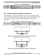
22.8.4 Reference Clock Pin Requirements
The OSC module requires use of both the EXTAL and XTAL pins to generate an output
clock in Oscillator mode, but requires only the EXTAL pin in External clock mode. The
EXTAL and XTAL pins are available for I/O. For the implementation of these pins on
this device, refer to the Signal Multiplexing chapter.
Chapter 22 Oscillator (OSC)
KL02 Sub-Family Reference Manual, Rev. 2.1, July 2013
Freescale Semiconductor, Inc.
295
Содержание KKL02Z32CAF4R
Страница 2: ...KL02 Sub Family Reference Manual Rev 2 1 July 2013 2 Freescale Semiconductor Inc...
Страница 24: ...KL02 Sub Family Reference Manual Rev 2 1 July 2013 24 Freescale Semiconductor Inc...
Страница 36: ...Orderable part numbers KL02 Sub Family Reference Manual Rev 2 1 July 2013 36 Freescale Semiconductor Inc...
Страница 76: ...Human machine interfaces HMI KL02 Sub Family Reference Manual Rev 2 1 July 2013 76 Freescale Semiconductor Inc...
Страница 94: ...Module clocks KL02 Sub Family Reference Manual Rev 2 1 July 2013 94 Freescale Semiconductor Inc...
Страница 142: ...Functional description KL02 Sub Family Reference Manual Rev 2 1 July 2013 142 Freescale Semiconductor Inc...
Страница 188: ...Memory map and register descriptions KL02 Sub Family Reference Manual Rev 2 1 July 2013 188 Freescale Semiconductor Inc...
Страница 214: ...Application information KL02 Sub Family Reference Manual Rev 2 1 July 2013 214 Freescale Semiconductor Inc...
Страница 222: ...Memory map register descriptions KL02 Sub Family Reference Manual Rev 2 1 July 2013 222 Freescale Semiconductor Inc...
Страница 256: ...Memory map and register definition KL02 Sub Family Reference Manual Rev 2 1 July 2013 256 Freescale Semiconductor Inc...
Страница 300: ...Functional description KL02 Sub Family Reference Manual Rev 2 1 July 2013 300 Freescale Semiconductor Inc...
Страница 532: ...Functional description KL02 Sub Family Reference Manual Rev 2 1 July 2013 532 Freescale Semiconductor Inc...
Страница 534: ...KL02 Sub Family Reference Manual Rev 2 1 July 2013 534 Freescale Semiconductor Inc...


