


1. The RESET_b pin has the passive analog filter fixed enabled when functioning as the RESET_b pin
(FTFA_FOPT[RESET_PIN_CFG] = 1) and fixed disabled when configured for other shared functions.
10.2.2 Clock gating
The clock to the port control module can be gated on and off using the SCGC5[PORTx]
bits in the SIM module. These bits are cleared after any reset, which disables the clock to
the corresponding module to conserve power. Prior to initializing the corresponding
module, set SIM_SCGC5[PORTx] to enable the clock. Before turning off the clock,
make sure to disable the module. For more details, see the
chapter.
10.2.3 Signal multiplexing constraints
1. A given peripheral function must be assigned to a maximum of one package pin. Do
not program the same function to more than one pin.
2. To ensure the best signal timing for a given peripheral's interface, choose the pins in
closest proximity to each other.
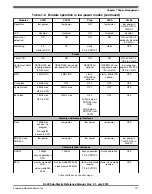
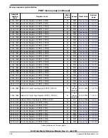
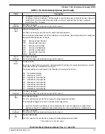
10.3 Pinout
10.3.1 KL02 signal multiplexing and pin assignments
The following table shows the signals available on each pin and the locations of these
pins on the devices supported by this document. The Port Control Module is responsible
for selecting which ALT functionality is available on each pin.
NOTE
PTB3 and PTB4 are true open drain pins. The external pullup
resistor must be added to make them output correct values in
using I2C, GPIO, and UART0.
20
WLC
SP
Pin Name
Default
ALT0
ALT1
ALT2
ALT3
B4
VDD
VDD
VDD
B4
VREFH
VREFH
VREFH
C3
VREFL
VREFL
VREFL
C3
VSS
VSS
VSS
C4
PTA3
EXTAL0
EXTAL0
PTA3
I2C0_SCL
I2C1_SDA
D4
PTA4
XTAL0
XTAL0
PTA4
I2C0_SDA
I2C1_SCL
Chapter 10 Signal Multiplexing and Signal Descriptions
KL02 Sub-Family Reference Manual, Rev. 2.1, July 2013
Freescale Semiconductor, Inc.
125
Содержание KKL02Z32CAF4R
Страница 2: ...KL02 Sub Family Reference Manual Rev 2 1 July 2013 2 Freescale Semiconductor Inc...
Страница 24: ...KL02 Sub Family Reference Manual Rev 2 1 July 2013 24 Freescale Semiconductor Inc...
Страница 36: ...Orderable part numbers KL02 Sub Family Reference Manual Rev 2 1 July 2013 36 Freescale Semiconductor Inc...
Страница 76: ...Human machine interfaces HMI KL02 Sub Family Reference Manual Rev 2 1 July 2013 76 Freescale Semiconductor Inc...
Страница 94: ...Module clocks KL02 Sub Family Reference Manual Rev 2 1 July 2013 94 Freescale Semiconductor Inc...
Страница 142: ...Functional description KL02 Sub Family Reference Manual Rev 2 1 July 2013 142 Freescale Semiconductor Inc...
Страница 188: ...Memory map and register descriptions KL02 Sub Family Reference Manual Rev 2 1 July 2013 188 Freescale Semiconductor Inc...
Страница 214: ...Application information KL02 Sub Family Reference Manual Rev 2 1 July 2013 214 Freescale Semiconductor Inc...
Страница 222: ...Memory map register descriptions KL02 Sub Family Reference Manual Rev 2 1 July 2013 222 Freescale Semiconductor Inc...
Страница 256: ...Memory map and register definition KL02 Sub Family Reference Manual Rev 2 1 July 2013 256 Freescale Semiconductor Inc...
Страница 300: ...Functional description KL02 Sub Family Reference Manual Rev 2 1 July 2013 300 Freescale Semiconductor Inc...
Страница 532: ...Functional description KL02 Sub Family Reference Manual Rev 2 1 July 2013 532 Freescale Semiconductor Inc...
Страница 534: ...KL02 Sub Family Reference Manual Rev 2 1 July 2013 534 Freescale Semiconductor Inc...


