45
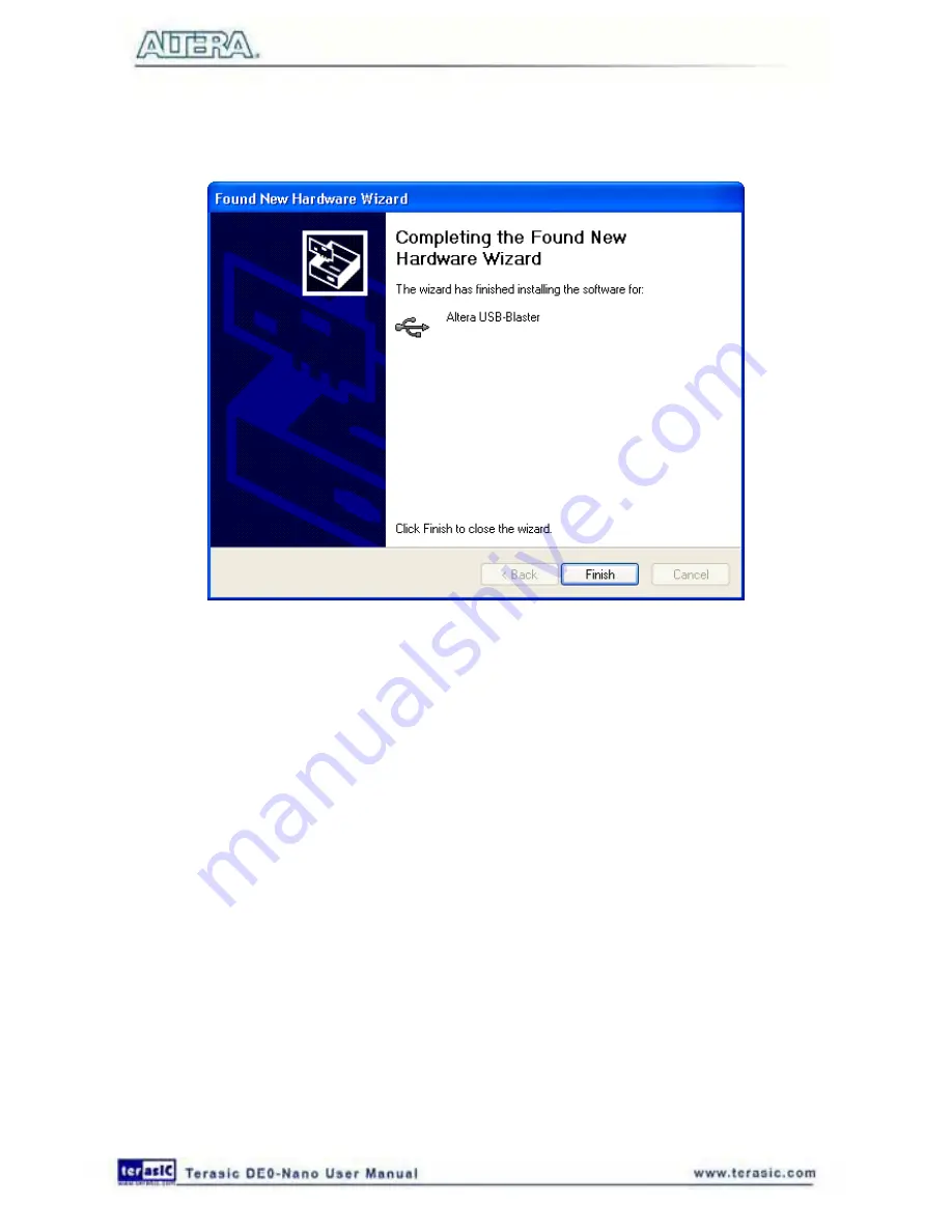
The driver will now be installed as indicated in
Figure 6-7
. Click
Finish
and you can start using the
DE0-Nano board.
Figure 6-7 The driver is installed
6
6
.
.
3
3
W
W
h
h
a
a
t
t
Y
Y
o
o
u
u
W
W
i
i
l
l
l
l
L
L
e
e
a
a
r
r
n
n
In this tutorial you will perform the following tasks:
Create a design that causes LEDs on the development board to blink at two distinct rates. This
design is easy to create and gives you visual feedback that the design works. Of course, you can use
your DE0-Nano board to run other designs as well. For the LED design, you will write Verilog HDL
code for a simple 32-bit counter, add a phase-locked loop (PLL) megafunction as the clock source,
and add a 2-input multiplexer megafunction. When the design is running on the board, you can
press an input switch to multiplex the counter bits that drive the output LEDs.
6
6
.
.
4
4
A
A
s
s
s
s
i
i
g
g
n
n
T
T
h
h
e
e
D
D
e
e
v
v
i
i
c
c
e
e
Begin this tutorial by creating a new Quartus II project. A project is a set of files that maintain
information about your FPGA design. The Quartus II Settings File (.qsf) and Quartus II Project File
(.qpf) files are the primary files in a Quartus II project. To compile a design or make pin
assignments, you must first create a project. The steps used to create a project are:
Summary of Contents for De0-Nano
Page 1: ...1 ...
Page 4: ...4 9 3 Revision History 155 9 4 Copyright Statement 155 ...
Page 44: ...44 Figure 6 5 Browse to find the location Figure 6 6 There is no need to test the driver ...
Page 90: ...90 Figure 7 14 Add NIOS II Processor ...
Page 93: ...93 Figure 7 17 Rename the CPU 1 Figure 7 18 Rename the CPU 2 ...
Page 98: ...98 Figure 7 23 Add On Chip Memory ...
Page 100: ...100 Figure 7 25 Update Total memory size ...
Page 102: ...102 Figure 7 28 Update CPU settings ...
Page 104: ...104 Figure 7 30 Add PIO ...
Page 106: ...106 Figure 7 32 PIO 21 Rename pio_0 to pio_led as shown in Figure 7 33 Figure 7 33 Rename PIO ...
Page 113: ...113 Figure 7 43 Input verilog Text Figure 7 44 Open DE0_NANO_SOPC v ...
Page 146: ...146 Figure 8 16 Display Progress and Result Information for the SDRAM Demonstration ...
Page 150: ...150 Figure 9 3 Select Devices Page ...
Page 151: ...151 Figure 9 4 Convert Programming Files Page ...


