37
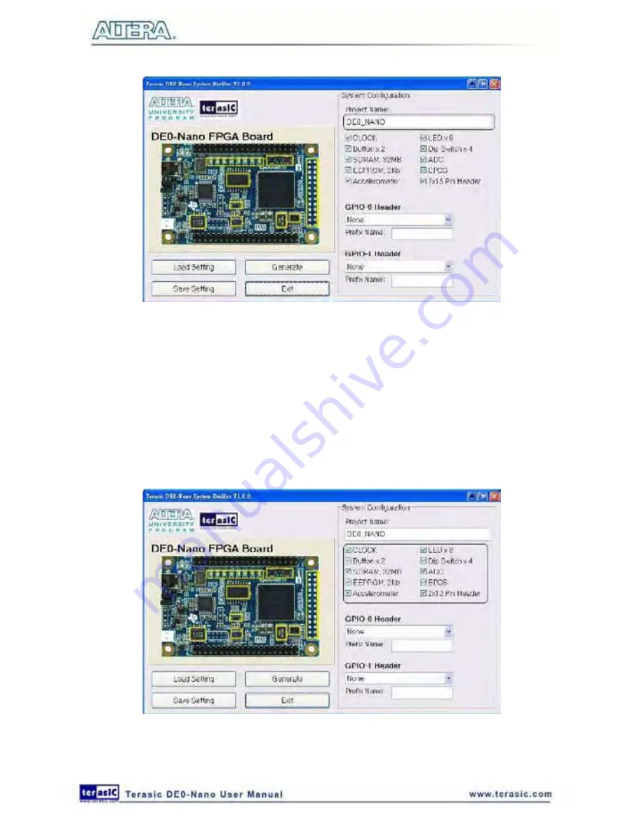
Figure 5-3 The DE0-Nano Board Type and Project Name
System Configuration
Under System Configuration users are given the flexibility of enabling their choice of included
components on the DE0-Nano as shown in
Figure 5-4
. Each component of the DE0-Nano is listed
where users can enable or disable a component according to their design by simply marking a check
or removing the check in the field provided. If the component is enabled, the DE0-Nano System
Builder will automatically generate the associated pin assignments including the pin name, pin
location, pin direction, and I/O standard.
Figure 5-4 System Configuration Group
GPIO Expansion
Summary of Contents for De0-Nano
Page 1: ...1 ...
Page 4: ...4 9 3 Revision History 155 9 4 Copyright Statement 155 ...
Page 44: ...44 Figure 6 5 Browse to find the location Figure 6 6 There is no need to test the driver ...
Page 90: ...90 Figure 7 14 Add NIOS II Processor ...
Page 93: ...93 Figure 7 17 Rename the CPU 1 Figure 7 18 Rename the CPU 2 ...
Page 98: ...98 Figure 7 23 Add On Chip Memory ...
Page 100: ...100 Figure 7 25 Update Total memory size ...
Page 102: ...102 Figure 7 28 Update CPU settings ...
Page 104: ...104 Figure 7 30 Add PIO ...
Page 106: ...106 Figure 7 32 PIO 21 Rename pio_0 to pio_led as shown in Figure 7 33 Figure 7 33 Rename PIO ...
Page 113: ...113 Figure 7 43 Input verilog Text Figure 7 44 Open DE0_NANO_SOPC v ...
Page 146: ...146 Figure 8 16 Display Progress and Result Information for the SDRAM Demonstration ...
Page 150: ...150 Figure 9 3 Select Devices Page ...
Page 151: ...151 Figure 9 4 Convert Programming Files Page ...


