70
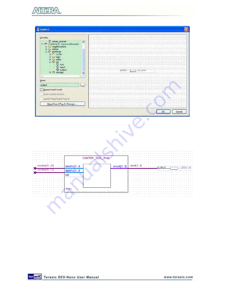
Figure 6-38 Choose output pin
18. Click
OK
.
19. Place this output pin so that it connects to the counter_bus_mux’s result [3..0] bus output line.
20. Rename the output pin as LED [3..0]. (see
Figure 6-39
).
Figure 6-39 Rename the output pin
21. Attach an input pin to the multiplexer select line using an input pin:
a. Right click in the blank area of the BDF and select
Insert > Symbol
.
b. Under Libraries, double-click quartus/libraries/ > primitives > pin > input.
c. Click
OK
.
22. Place this input pin below
counter_bus_mux
.
23. Connect the input pin to the
counter_bus_mux
sel pin.
24. Rename the input pin as KEY [0] (see
Figure 6-40
).
Summary of Contents for De0-Nano
Page 1: ...1 ...
Page 4: ...4 9 3 Revision History 155 9 4 Copyright Statement 155 ...
Page 44: ...44 Figure 6 5 Browse to find the location Figure 6 6 There is no need to test the driver ...
Page 90: ...90 Figure 7 14 Add NIOS II Processor ...
Page 93: ...93 Figure 7 17 Rename the CPU 1 Figure 7 18 Rename the CPU 2 ...
Page 98: ...98 Figure 7 23 Add On Chip Memory ...
Page 100: ...100 Figure 7 25 Update Total memory size ...
Page 102: ...102 Figure 7 28 Update CPU settings ...
Page 104: ...104 Figure 7 30 Add PIO ...
Page 106: ...106 Figure 7 32 PIO 21 Rename pio_0 to pio_led as shown in Figure 7 33 Figure 7 33 Rename PIO ...
Page 113: ...113 Figure 7 43 Input verilog Text Figure 7 44 Open DE0_NANO_SOPC v ...
Page 146: ...146 Figure 8 16 Display Progress and Result Information for the SDRAM Demonstration ...
Page 150: ...150 Figure 9 3 Select Devices Page ...
Page 151: ...151 Figure 9 4 Convert Programming Files Page ...


