71
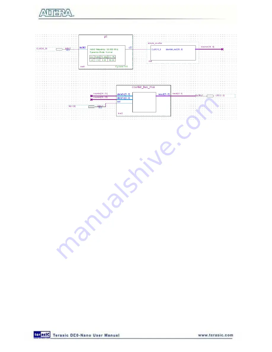
Figure 6-40 Adding the KEY [0] Input Pin
You have finished adding all required components of the circuit to your design. You can add notes
or information to the project as text using the Text tool on the toolbar (indicated with the A symbol).
For example, you can add the label “OFF = SLOW, ON = FAST” to the KEY [0] input pin and add
a project description, such as “DE0-Nano Tutorial Project.”
6
6
.
.
6
6
A
A
s
s
s
s
i
i
g
g
n
n
t
t
h
h
e
e
P
P
i
i
n
n
s
s
In this section, you will make pin assignments. Before making pin assignments, perform the
following steps:
1. Select
Processing > Start > Start Analysis & Elaboration
in preparation for assigning pin
locations.
2. Click
OK
in the message window that appears after analysis and elaboration completes.
To make pin assignments to the KEY [0] and CLOCK_50 input pins and to the LED[3..0] output
pins, perform the following steps:
1. Select
Assignments > Pin Planner
, which opens the Pin Planner, a spreadsheet-like table of
specific pin assignments. The Pin Planner shows the design’s six pins. See
Figure 6-41
Summary of Contents for De0-Nano
Page 1: ...1 ...
Page 4: ...4 9 3 Revision History 155 9 4 Copyright Statement 155 ...
Page 44: ...44 Figure 6 5 Browse to find the location Figure 6 6 There is no need to test the driver ...
Page 90: ...90 Figure 7 14 Add NIOS II Processor ...
Page 93: ...93 Figure 7 17 Rename the CPU 1 Figure 7 18 Rename the CPU 2 ...
Page 98: ...98 Figure 7 23 Add On Chip Memory ...
Page 100: ...100 Figure 7 25 Update Total memory size ...
Page 102: ...102 Figure 7 28 Update CPU settings ...
Page 104: ...104 Figure 7 30 Add PIO ...
Page 106: ...106 Figure 7 32 PIO 21 Rename pio_0 to pio_led as shown in Figure 7 33 Figure 7 33 Rename PIO ...
Page 113: ...113 Figure 7 43 Input verilog Text Figure 7 44 Open DE0_NANO_SOPC v ...
Page 146: ...146 Figure 8 16 Display Progress and Result Information for the SDRAM Demonstration ...
Page 150: ...150 Figure 9 3 Select Devices Page ...
Page 151: ...151 Figure 9 4 Convert Programming Files Page ...


