38
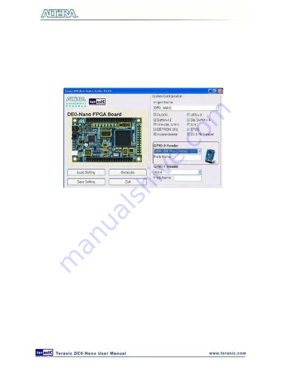
Users can connect GPIO expansion card onto GPIO header located on the DE0-Nano board as
shown in
Figure 5-5
. Select the appropriate daughter card you wish to include in your design from
the drop-down menu. The system builder will automatically generate the associated pin assignments
including the pin name, pin location, pin direction, and IO standard.
If a customized daughter board is used, users can select “GPIO Default” followed by changing the
pin name and pin direction according to the specification of the customized daughter board.
Figure 5-5 GPIO Expansion Group
The “Prefix Name” is an optional feature which denotes the prefix pin name of the daughter card
assigned in your design. Users may leave this field empty.
Project Setting Management
The DE0-Nano System Builder also provides functions to restore default setting, loading a setting,
and saving users’ board configuration file shown in
Figure 5-6
. Users can save the current board
configuration information into a .cfg file and load it to the DE0-Nano System Builder.
Summary of Contents for De0-Nano
Page 1: ...1 ...
Page 4: ...4 9 3 Revision History 155 9 4 Copyright Statement 155 ...
Page 44: ...44 Figure 6 5 Browse to find the location Figure 6 6 There is no need to test the driver ...
Page 90: ...90 Figure 7 14 Add NIOS II Processor ...
Page 93: ...93 Figure 7 17 Rename the CPU 1 Figure 7 18 Rename the CPU 2 ...
Page 98: ...98 Figure 7 23 Add On Chip Memory ...
Page 100: ...100 Figure 7 25 Update Total memory size ...
Page 102: ...102 Figure 7 28 Update CPU settings ...
Page 104: ...104 Figure 7 30 Add PIO ...
Page 106: ...106 Figure 7 32 PIO 21 Rename pio_0 to pio_led as shown in Figure 7 33 Figure 7 33 Rename PIO ...
Page 113: ...113 Figure 7 43 Input verilog Text Figure 7 44 Open DE0_NANO_SOPC v ...
Page 146: ...146 Figure 8 16 Display Progress and Result Information for the SDRAM Demonstration ...
Page 150: ...150 Figure 9 3 Select Devices Page ...
Page 151: ...151 Figure 9 4 Convert Programming Files Page ...


