76
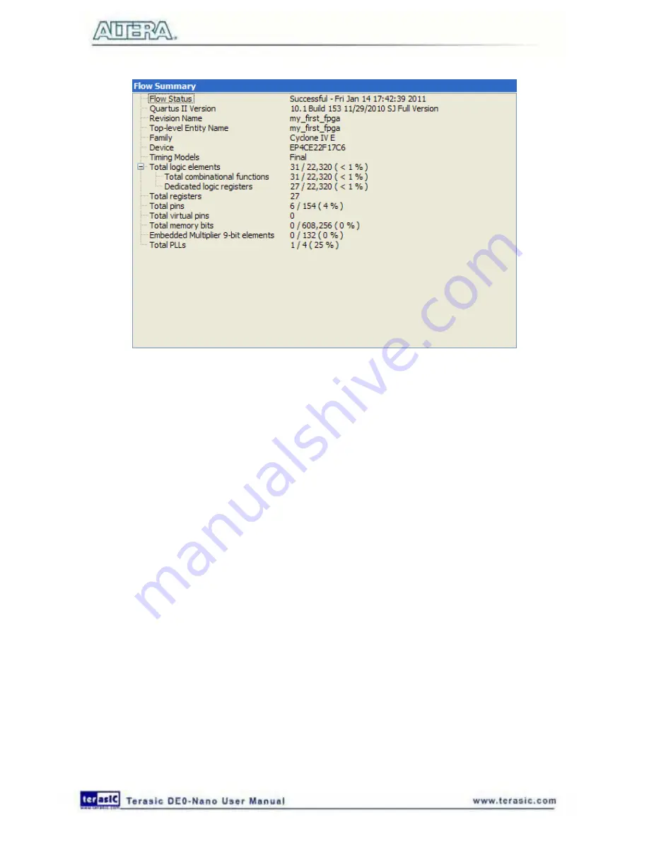
Figure 6-45 Compilation Report Example
6
6
.
.
9
9
P
P
r
r
o
o
g
g
r
r
a
a
m
m
t
t
h
h
e
e
F
F
P
P
G
G
A
A
D
D
e
e
v
v
i
i
c
c
e
e
After compiling and verifying your design you are ready to program the FPGA on the development
board. You download the SOF you just created into the FPGA using the USB-Blaster circuitry on
the board. Set up your hardware for programming using the following steps:
First, connect the USB cable, which was included in your development kit, between the DE0-Nano
and the host computer. Refer to the getting started user guide for detailed instructions on how to
connect the cables.
Refer to the getting started user guide for detailed instructions on how to connect the cables.
Program the FPGA using the following steps.
1. Select Tools > Programmer. The Programmer window opens, as shown in
Figure 6-46
.
Summary of Contents for De0-Nano
Page 1: ...1 ...
Page 4: ...4 9 3 Revision History 155 9 4 Copyright Statement 155 ...
Page 44: ...44 Figure 6 5 Browse to find the location Figure 6 6 There is no need to test the driver ...
Page 90: ...90 Figure 7 14 Add NIOS II Processor ...
Page 93: ...93 Figure 7 17 Rename the CPU 1 Figure 7 18 Rename the CPU 2 ...
Page 98: ...98 Figure 7 23 Add On Chip Memory ...
Page 100: ...100 Figure 7 25 Update Total memory size ...
Page 102: ...102 Figure 7 28 Update CPU settings ...
Page 104: ...104 Figure 7 30 Add PIO ...
Page 106: ...106 Figure 7 32 PIO 21 Rename pio_0 to pio_led as shown in Figure 7 33 Figure 7 33 Rename PIO ...
Page 113: ...113 Figure 7 43 Input verilog Text Figure 7 44 Open DE0_NANO_SOPC v ...
Page 146: ...146 Figure 8 16 Display Progress and Result Information for the SDRAM Demonstration ...
Page 150: ...150 Figure 9 3 Select Devices Page ...
Page 151: ...151 Figure 9 4 Convert Programming Files Page ...


