


LH75400/01/10/11 (Preliminary) User’s Guide
Timers
6/17/03
15-7
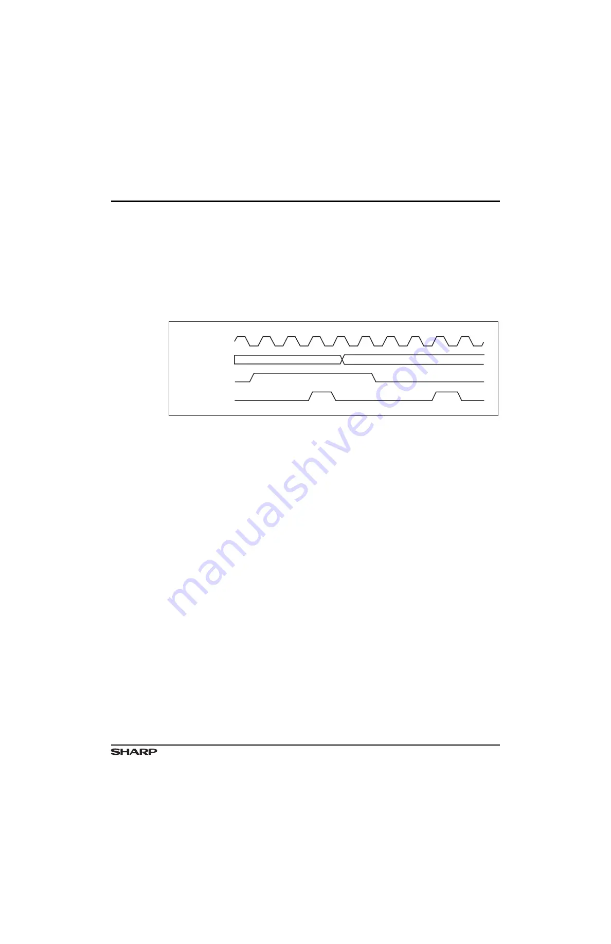
15.1.3 Capture Signal Sampling
The capture signal is sampled on the rising edge of the system clock. The pulse width of a
capture signal must be equal to or longer than two system clock periods plus, the setup time
for the signal to be correctly read in. After sampling, the external capture signal is synchro-
nized to the rising edge of the system clock. This synchronization process takes two system
clock periods. After the external capture signal is synchronized, the value of the counter is
stored in the appropriate CAP(n) Registers. The external capture signal is edge-selectable
and can use a rising or falling edge to capture the counter value.
15.1.4 PWM Mode
The timers support a Pulse Width Modulator (PWM) Mode. This mode uses the two Timer
Compare Registers associated with a timer to create a PWM. In this mode, the PWM signal
is output through CTCMP(n)A.
To enable PWM Mode for a timer, set the PWM bit in the appropriate Timer Control Reg-
ister to 1. If PWM Mode is enabled, set bit TC of the same Timer Control Register to 1. This
setting clears the counter when the Timer Control Register value matches the CMP1
value. The state of CTCMPnA matches the value of CMP1 starting from the time the
counter matches the CMP1 Register until it matches the CMP0 Register. The state of
CTCMP(n)A then matches the value of CMP0.
To create a proper PWM, set the CMP0 bit of the Timer Control Register opposite to the
setting for the CMP1 bit. For example, if CMP1 of the CMP_CAP_CTRL Register is set to
10 (output 1 to CTCMP0B), CMP0 of the same register must be set to 01 (output 0 to
CTCMP0A). Failing to follow this requirement results in a steady logic 1 or 0.
In PWM Mode, PWM CTCMP(n)B remains at the logic level (1 or 0) programmed into the
CMP0 bits. When programming the compare values, the CMP1 Register must always be
greater than the CMP0 Register to create a PWM signal.
• The value in CMP1 Register is the period of the PWM plus one.
• The value in CMP0 is the duty cycle of the PWM plus one.
The PWM is clocked by the internal count clock, which is the prescaled system clock.
Figure 15-7. Capture Signal Synchronization Timing
SYSTEM
CLOCK
EDGE
SELECTION
EXTERNAL
CAPTURE SIGNAL
RISING
FALLING
CAPTURE SIGNAL
AFTER SAMPLING
LH754xx-22