


MOTOROLA CMOS LOGIC DATA
6–57
MC14017B
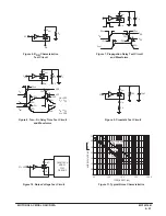
Figure 1. Typical Output Source and Output Sink Characteristics Test Circuit
VDD
Vout
VSS
VDD
VSS
S1
S1
A
B
VSS
ID
EXTERNAL
POWER
SUPPLY
CLOCK
ENABLE
RESET
CLOCK Cout
Q0
Q1
Q2
Q3
Q4
Q5
Q6
Q7
Q8
Q9
Output
Sink Drive
Output
Source Drive
Decode
Outputs
Clock to
desired
outputs
(S1 to B)
(S1 to A)
Carry
Clock to 5
thru 9
(S1 to B)
S1 to A
VGS =
– VDD
VDD
VDS =
Vout – VDD
Vout
Figure 2. Typical Power Dissipation Test Circuit
VDD
VSS
ID
CLOCK
ENABLE
RESET
CLOCK
Cout
Q0
Q1
Q2
Q3
Q4
Q5
Q6
Q7
Q8
Q9
500
µ
F
0.01
µ
F
CERAMIC
PULSE
GENERATOR
fc
CL
CL
CL
CL
CL
CL
CL
CL
CL
CL
CL
APPLICATIONS INFORMATION
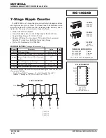
Figure 3 shows a technique for extending the number of decoded output states for the MC14017B. Decoded outputs are se-
quential within each stage and from stage to stage, with no dead time (except propagation delay).
Figure 3. Counter Expansion
RESET
CLOCK
CE
MC14017B
Q0 Q1
Q8 Q9
• • •
9 DECODED
OUTPUTS
CLOCK
FIRST STAGE
INTERMEDIATE STAGES
LAST STAGE
RESET
CLOCK
CE
MC14017B
Q0Q1
Q8 Q9
• • •
RESET
CLOCK
CE
MC14017B
Q1
Q8 Q9
• • •
8 DECODED
OUTPUTS
8 DECODED
OUTPUTS
Summary of Contents for CMOS Logic
Page 1: ......
Page 5: ...iv MOTOROLA CMOS LOGIC DATA ...
Page 6: ...Master Index 1 ...
Page 12: ...Product Selection Guide 2 ...
Page 17: ...The Better Program 3 ...
Page 20: ...B and UB Series Family Data 4 ...
Page 25: ...CMOS Handling and Design Guidelines 5 ...
Page 32: ...CMOS Handling and Design Guidelines 5 ...
Page 39: ...Data Sheets 6 ...
Page 234: ...MOTOROLA CMOS LOGIC DATA MC14174B 6 196 FUNCTIONAL BLOCK DIAGRAM TIMING DIAGRAM ...
Page 238: ...MOTOROLA CMOS LOGIC DATA MC14175B 6 200 FUNCTIONAL BLOCK DIAGRAM TIMING DIAGRAM ...
Page 555: ...CMOS Reliability 7 ...
Page 561: ...Equivalent Gate Count 8 ...
Page 563: ...Packaging Information Including Surface Mounts 9 ...
Page 571: ......