


MOTOROLA CMOS LOGIC DATA
6–221
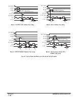
MC14500B
TIMING WAVEFORMS
Instructions
NOPO, NOPF
Instructions
RR, IEN, OEN remain unaffected
Instructions
SKZ, JMP, RTN
Instructions
RR, IEN, OEN remain unaffected
X1
RST
IEN
REGISTER
OEN
REGISTER
RR
4–BIT
INSTRUCTION
FLAG 0
FLAG F
tW(R)
tPHL
(RESET TO XI)
tPHL (RESET TO RR)
NOP0
NOPF
NOPO
tPLH
(DATA TO FLAG)
tPHL
X1
4–BIT
INSTRUCTION
RST
RR
JMP FLAG
RTN FLAG
SKP F/F
INTERNAL
* Instructions Ignored.
tW(cl)
SKZ
*
JMP
RTN
*
JMP
tPHL
(RESET TO JUMP)
Summary of Contents for CMOS Logic
Page 1: ......
Page 5: ...iv MOTOROLA CMOS LOGIC DATA ...
Page 6: ...Master Index 1 ...
Page 12: ...Product Selection Guide 2 ...
Page 17: ...The Better Program 3 ...
Page 20: ...B and UB Series Family Data 4 ...
Page 25: ...CMOS Handling and Design Guidelines 5 ...
Page 32: ...CMOS Handling and Design Guidelines 5 ...
Page 39: ...Data Sheets 6 ...
Page 234: ...MOTOROLA CMOS LOGIC DATA MC14174B 6 196 FUNCTIONAL BLOCK DIAGRAM TIMING DIAGRAM ...
Page 238: ...MOTOROLA CMOS LOGIC DATA MC14175B 6 200 FUNCTIONAL BLOCK DIAGRAM TIMING DIAGRAM ...
Page 555: ...CMOS Reliability 7 ...
Page 561: ...Equivalent Gate Count 8 ...
Page 563: ...Packaging Information Including Surface Mounts 9 ...
Page 571: ......