


MOTOROLA CMOS LOGIC DATA
6–367
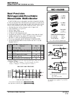
MC14538B
ÎÎÎÎÎÎÎÎÎÎÎÎÎÎÎÎÎÎÎÎÎÎÎÎÎÎÎÎÎÎÎÎÎÎ
ÎÎÎÎÎÎÎÎÎÎÎÎÎÎÎÎÎÎÎÎÎÎÎÎÎÎÎÎÎÎÎÎÎÎ
SWITCHING CHARACTERISTICS*
(CL = 50 pF, TA = 25
_
C)
VDD
All Types
Characteristic
Symbol
VDD
Vdc
Min
Typ #
Max
Unit
Output Rise Time
tTLH = (1.35 ns/pF) CL + 33 ns
tTLH = (0.60 ns/pF) CL + 20 ns
tTLH = (0.40 ns/pF) CL + 20 ns
tTLH
5.0
10
15
—
—
—
100
50
40
200
100
80
ns
Output Fall Time
tTHL = (1.35 ns/pF) CL + 33 ns
tTHL = (0.60 ns/pF) CL + 20 ns
tTHL = (0.40 ns/pF) CL + 20 ns
tTHL
5.0
10
15
—
—
—
100
50
40
200
100
80
ns
Propagation Delay Time
A or B to Q or Q
tPLH, tPHL = (0.90 ns/pF) CL + 255 ns
tPLH, tPHL = (0.36 ns/pF) CL + 132 ns
tPLH, tPHL = (0.26 ns/pF) CL + 87 ns
tPLH,
tPHL
5.0
10
15
—
—
—
300
150
100
600
300
220
ns
Reset to Q or Q
tPLH, tPHL = (0.90 ns/pF) CL + 205 ns
tPLH, tPHL = (0.36 ns/pF) CL + 107 ns
tPLH, tPHL = (0.26 ns/pF) CL + 82 ns
5.0
10
15
—
—
—
250
125
95
500
250
190
ns
Input Rise and Fall Times
Reset
tr, tf
5
10
15
—
—
—
—
—
—
15
5
4
µ
s
B Input
5
10
15
—
—
—
300
1.2
0.4
1.0
0.1
0.05
ms
A Input
5
10
15
No Limit
—
Input Pulse Width
A, B, or Reset
tWH,
tWL
5.0
10
15
170
90
80
85
45
40
—
—
—
ns
Retrigger Time
trr
5.0
10
15
0
0
0
—
—
—
—
—
—
ns
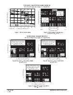
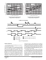
Output Pulse Width — Q or Q
Refer to Figures 8 and 9
CX = 0.002
µ
F, RX = 100 k
Ω
T
5.0
10
15
198
200
202
210
212
214
230
232
234
µ
s
CX = 0.1
µ
F, RX = 100 k
Ω
5.0
10
15
9.3
9.4
9.5
9.86
10
10.14
10.5
10.6
10.7
ms
CX = 10
µ
F, RX = 100 k
Ω
5.0
10
15
0.91
0.92
0.93
0.965
0.98
0.99
1.03
1.04
1.06
s
Pulse Width Match between circuits in
the same package.
CX = 0.1
µ
F, RX = 100 k
Ω
100
[(T1 – T2)/T1]
5.0
10
15
—
—
—
±
1.0
±
1.0
±
1.0
±
5.0
±
5.0
±
5.0
%
* The formulas given are for the typical characteristics only at 25
_
C.
#Data labelled “Typ” is not to be used for design purposes but is intended as an indication of the IC’s potential performance.
ÎÎÎÎÎÎÎÎÎÎÎÎÎÎÎÎÎÎÎÎÎÎÎÎÎÎÎÎÎÎÎÎÎÎ
ÎÎÎÎÎÎÎÎÎÎÎÎÎÎÎÎÎÎÎÎÎÎÎÎÎÎÎÎÎÎÎÎÎÎ
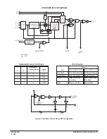
OPERATING CONDITIONS
External Timing Resistance
RX
—
5.0
—
k
Ω
External Timing Capacitance
CX
—
0
—
No
Limit†
µ
F
* The maximum usable resistance RX is a function of the leakage of the capacitor CX, leakage of the MC14538B, and leakage due to board layout
and surface resistance. Susceptibility to externally induced noise signals may occur for RX > 1 M
Ω
..
†If CX > 15
µ
F, use discharge protection diode per Fig. 11.
Summary of Contents for CMOS Logic
Page 1: ......
Page 5: ...iv MOTOROLA CMOS LOGIC DATA ...
Page 6: ...Master Index 1 ...
Page 12: ...Product Selection Guide 2 ...
Page 17: ...The Better Program 3 ...
Page 20: ...B and UB Series Family Data 4 ...
Page 25: ...CMOS Handling and Design Guidelines 5 ...
Page 32: ...CMOS Handling and Design Guidelines 5 ...
Page 39: ...Data Sheets 6 ...
Page 234: ...MOTOROLA CMOS LOGIC DATA MC14174B 6 196 FUNCTIONAL BLOCK DIAGRAM TIMING DIAGRAM ...
Page 238: ...MOTOROLA CMOS LOGIC DATA MC14175B 6 200 FUNCTIONAL BLOCK DIAGRAM TIMING DIAGRAM ...
Page 555: ...CMOS Reliability 7 ...
Page 561: ...Equivalent Gate Count 8 ...
Page 563: ...Packaging Information Including Surface Mounts 9 ...
Page 571: ......