


MOTOROLA CMOS LOGIC DATA
MC14512B
6–262
8-Channel Data Selector
The MC14512B is an 8–channel data selector constructed with MOS
P–channel and N–channel enhancement mode devices in a single
monolithic structure. This data selector finds primary application in signal
multiplexing functions. It may also be used for data routing, digital signal
switching, signal gating, and number sequence generation.
•
Diode Protection on All Inputs
•
Single Supply Operation
•
3–State Output (Logic “1”, Logic “0”, High Impedance)
•
Supply Voltage Range = 3.0 Vdc to 18 Vdc
•
Capable of Driving Two Low–power TTL Loads or One Low–power
Schottky TTL Load Over the Rated Temperature Range
ÎÎÎÎÎÎÎÎÎÎÎÎÎÎÎÎÎÎÎÎÎ
ÎÎÎÎÎÎÎÎÎÎÎÎÎÎÎÎÎÎÎÎÎ
MAXIMUM RATINGS*
(Voltages Referenced to VSS)
Symbol
Parameter
Value
Unit
VDD
DC Supply Voltage
– 0.5 to + 18.0
V
Vin, Vout Input or Output Voltage (DC or Transient)
– 0.5 to VDD + 0.5
V
Iin, Iout
Input or Output Current (DC or Transient),
per Pin
±
10
mA
PD
Power Dissipation, per Package†
500
mW
Tstg
Storage Temperature
– 65 to + 150
_
C
TL
Lead Temperature (8–Second Soldering)
260
_
C
* Maximum Ratings are those values beyond which damage to the device may occur.
†Temperature Derating:
Plastic “P and D/DW” Packages: – 7.0 mW/
_
C From 65
_
C To 125
_
C
Ceramic “L” Packages: – 12 mW/
_
C From 100
_
C To 125
_
C
TRUTH TABLE
C
B
A
Inhibit
Disable
Z
0
0
0
0
0
X0
0
0
1
0
0
X1
0
1
0
0
0
X2
0
1
1
0
0
X3
1
0
0
0
0
X4
1
0
1
0
0
X5
1
1
0
0
0
X6
1
1
1
0
0
X7
X
X
X
1
0
0
X
X
X
X
1
High
Impedance
X = Don’t Care
MOTOROLA
SEMICONDUCTOR TECHNICAL DATA
MC14512B
L SUFFIX
CERAMIC
CASE 620
ORDERING INFORMATION
MC14XXXBCP
Plastic
MC14XXXBCL
Ceramic
MC14XXXBD
SOIC
TA = – 55
°
to 125
°
C for all packages.
P SUFFIX
PLASTIC
CASE 648
D SUFFIX
SOIC
CASE 751B
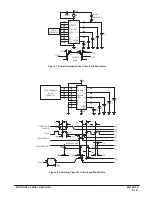
PIN ASSIGNMENT
This device contains protection circuitry to
guard against damage due to high static
voltages or electric fields. However, pre-
cautions must be taken to avoid applications of
any voltage higher than maximum rated volt-
ages to this high–impedance circuit. For proper
operation, Vin and Vout should be constrained
to the range VSS
v
(Vin or Vout)
v
VDD.
Unused inputs must always be tied to an
appropriate logic voltage level (e.g., either VSS
or VDD). Unused outputs must be left open.
13
14
15
16
9
10
11
12
5
4
3
2
1
8
7
6
B
C
Z
DIS
VDD
X7
INH
A
X3
X2
X1
X0
VSS
X6
X5
X4
Summary of Contents for CMOS Logic
Page 1: ......
Page 5: ...iv MOTOROLA CMOS LOGIC DATA ...
Page 6: ...Master Index 1 ...
Page 12: ...Product Selection Guide 2 ...
Page 17: ...The Better Program 3 ...
Page 20: ...B and UB Series Family Data 4 ...
Page 25: ...CMOS Handling and Design Guidelines 5 ...
Page 32: ...CMOS Handling and Design Guidelines 5 ...
Page 39: ...Data Sheets 6 ...
Page 234: ...MOTOROLA CMOS LOGIC DATA MC14174B 6 196 FUNCTIONAL BLOCK DIAGRAM TIMING DIAGRAM ...
Page 238: ...MOTOROLA CMOS LOGIC DATA MC14175B 6 200 FUNCTIONAL BLOCK DIAGRAM TIMING DIAGRAM ...
Page 555: ...CMOS Reliability 7 ...
Page 561: ...Equivalent Gate Count 8 ...
Page 563: ...Packaging Information Including Surface Mounts 9 ...
Page 571: ......