


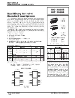


MOTOROLA CMOS LOGIC DATA
MC14554B
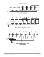
6–418
2-Bit by 2-Bit Parallel
Binary Multiplier
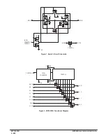
The MC14554B 2 x 2–bit parallel binary multiplier is constructed with
complementary MOS (CMOS) enhancement mode devices. The multiplier
can perform the multiplication of two binary numbers and simultaneously add
two other binary numbers to the product. The MC14554B has two
multiplicand inputs (X0 and X1), two multiplier inputs (Y0 and Y1), five
cascading or adding inputs (K0, K1, M0, M1, and M2), and five sum and
carry outputs (S0, S1, S2, C1 [S3], and C0). The basic multiplier can be
expanded into a straightforward m–bit by n–bit parallel multiplier without
additional logic elements.
Application areas include arithmetic processing (multiplying/adding,
obtaining square roots, polynomial evaluation, obtaining reciprocals, and
dividing), Fast Fourier Transform processing, digital filtering, communica-
tions (convolution and correlation), and process and machine controls.
•
Diode Protection on All Inputs
•
All Outputs Buffered
•
Straight–forward m–Bit By n–Bit Expansion
•
No Additional Logic Elements Needed for Expansion
•
Multiplies and Adds Simultaneously
•
Positive Logic Design
•
Supply Voltage Range = 3.0 Vdc to 18 Vdc
•
Capable of Driving Two Low–Power TTL Loads or One Low–Power
Schottky TTL Load Over the Rated Temperature Range
ÎÎÎÎÎÎÎÎÎÎÎÎÎÎÎÎÎÎÎÎÎ
ÎÎÎÎÎÎÎÎÎÎÎÎÎÎÎÎÎÎÎÎÎ
MAXIMUM RATINGS*
(Voltages Referenced to VSS)
Symbol
Parameter
Value
Unit
VDD
DC Supply Voltage
– 0.5 to + 18.0
V
Vin, Vout Input or Output Voltage (DC or Transient)
– 0.5 to VDD + 0.5
V
Iin, Iout
Input or Output Current (DC or Transient),
per Pin
±
10
mA
PD
Power Dissipation, per Package†
500
mW
Tstg
Storage Temperature
– 65 to + 150
_
C
TL
Lead Temperature (8–Second Soldering)
260
_
C
* Maximum Ratings are those values beyond which damage to the device may occur.
†Temperature Derating:
Plastic “P and D/DW” Packages: – 7.0 mW/
_
C From 65
_
C To 125
_
C
Ceramic “L” Packages: – 12 mW/
_
C From 100
_
C To 125
_
C
PIN ASSIGNMENT
13
14
15
16
9
10
11
12
5
4
3
2
1
8
7
6
K0
X1
X0
Y0
VDD
S1
K1
S0
C0
M1
M0
Y1
VSS
S2
C1 (S3)
M2
MOTOROLA
SEMICONDUCTOR TECHNICAL DATA
MC14554B
This device contains protection circuitry to
guard against damage due to high static
voltages or electric fields. However, pre-
cautions must be taken to avoid applications of
any voltage higher than maximum rated volt-
ages to this high–impedance circuit. For proper
operation, Vin and Vout should be constrained
to the range VSS
v
(Vin or Vout)
v
VDD.
Unused inputs must always be tied to an
appropriate logic voltage level (e.g., either VSS
or VDD). Unused outputs must be left open.
L SUFFIX
CERAMIC
CASE 620
ORDERING INFORMATION
MC14XXXBCP
Plastic
MC14XXXBCL
Ceramic
MC14XXXBD
SOIC
TA = – 55
°
to 125
°
C for all packages.
P SUFFIX
PLASTIC
CASE 648
D SUFFIX
SOIC
CASE 751B
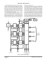
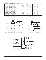
S = (X x Y) + K + M
Where:
x Means Arithmetic Times.
+ Means Arithmetic Plus.
S = S3 S2 S1 S0, X = X1X0, Y = Y1Y0,
K = K1 K0, M = M1 M0 (Binary Numbers).
Example:
Given: X = 2(1), Y = 3(11)
K = 1(01), M = 2(10)
Then:
S = (2 x 3) + 1 + 2 = 9
S = (10 x 11) + 01 + 10 = 1001
EQUATIONS
NOTE: C0 connected to M2 for this size
multiplier. See general expansion
diagram for other size multipliers.
Summary of Contents for CMOS Logic
Page 1: ......
Page 5: ...iv MOTOROLA CMOS LOGIC DATA ...
Page 6: ...Master Index 1 ...
Page 12: ...Product Selection Guide 2 ...
Page 17: ...The Better Program 3 ...
Page 20: ...B and UB Series Family Data 4 ...
Page 25: ...CMOS Handling and Design Guidelines 5 ...
Page 32: ...CMOS Handling and Design Guidelines 5 ...
Page 39: ...Data Sheets 6 ...
Page 234: ...MOTOROLA CMOS LOGIC DATA MC14174B 6 196 FUNCTIONAL BLOCK DIAGRAM TIMING DIAGRAM ...
Page 238: ...MOTOROLA CMOS LOGIC DATA MC14175B 6 200 FUNCTIONAL BLOCK DIAGRAM TIMING DIAGRAM ...
Page 555: ...CMOS Reliability 7 ...
Page 561: ...Equivalent Gate Count 8 ...
Page 563: ...Packaging Information Including Surface Mounts 9 ...
Page 571: ......