


MOTOROLA CMOS LOGIC DATA
6–399
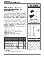
MC14549B MC14559B
ÎÎÎÎÎÎÎÎÎÎÎÎÎÎÎÎÎÎÎÎÎÎÎÎÎÎÎÎÎÎÎÎÎÎ
ÎÎÎÎÎÎÎÎÎÎÎÎÎÎÎÎÎÎÎÎÎÎÎÎÎÎÎÎÎÎÎÎÎÎ
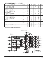
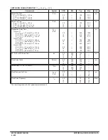
ELECTRICAL CHARACTERISTICS
(Voltages Referenced to VSS)
VDD
– 55
_
C
25
_
C
125
_
C
Characteristic
Symbol
Vdc
Min
Max
Min
Typ #
Max
Min
Max
Unit
Output Voltage
“0” Level
Vin = VDD or 0
VOL
5.0
10
15
—
—
—
0.05
0.05
0.05
—
—
—
0
0
0
0.05
0.05
0.05
—
—
—
0.05
0.05
0.05
Vdc
“1” Level
Vin = 0 or VDD
VOH
5.0
10
15
4.95
9.95
14.95
—
—
—
4.95
9.95
14.95
5.0
10
15
—
—
—
4.95
9.95
14.95
—
—
—
Vdc
Input Voltage #
“0” Level
(VO = 4.5 or 0.5 Vdc)
(VO = 9.0 or 1.0 Vdc)
(VO = 13.5 or 1.5 Vdc)
VIL
5.0
10
15
—
—
—
1.5
3.0
4.0
—
—
—
2.25
4.50
6.75
1.5
3.0
4.0
—
—
—
1.5
3.0
4.0
Vdc
“1” Level
(VO = 0.5 or 4.5 Vdc)
(VO = 1.0 or 9.0 Vdc)
(VO = 1.5 or 13.5 Vdc)
VIH
5.0
10
15
3.5
7.0
11
—
—
—
3.5
7.0
11
2.75
5.50
8.25
—
—
—
3.5
7.0
11
—
—
—
Vdc
Output Drive Current
(VOH = 2.5 Vdc)
Source
(VOH = 4.6 Vdc)
(VOH = 9.5 Vdc)
(VOH = 13.5 Vdc)
IOH
5.0
5.0
10
15
– 1.2
– 0.25
– 0.62
– 1.8
—
—
—
—
– 1.0
– 0.2
– 0.5
– 1.5
– 1.7
– 0.36
– 0.9
– 3.5
—
—
—
—
– 0.7
– 0.14
– 0.35
– 1.1
—
—
—
—
mAdc
(VOL = 0.4 Vdc)
Sink
(VOL = 0.5 Vdc)
Q Outputs
(VOL = 1.5 Vdc)
IOL
5.0
10
15
1.28
3.2
8.4
—
—
—
1.02
2.6
6.8
1.76
4.5
17.6
—
—
—
0.72
1.8
4.8
—
—
—
mAdc
(VOL = 0.4 Vdc)
Sink
(VOL = 0.5 Vdc)
Pin 5, 11 only
(VOL = 1.5 Vdc)
5.0
10
15
0.64
1.6
4.2
—
—
—
0.51
1.3
3.4
0.88
2.25
8.8
—
—
—
0.36
0.9
2.4
—
—
—
mAdc
Input Current
Iin
15
—
±
0.1
—
±
0.00001
±
0.1
—
±
1.0
µ
Adc
Input Capacitance
Cin
—
—
—
—
5.0
7.5
—
—
pF
Quiescent Current
(Per Package)
(Clock = 0 V,
Other Inputs = VDD
or 0 V, Iout = 0
µ
A)
IDD
5.0
10
15
—
—
—
5.0
10
20
—
—
—
0.005
0.010
0.015
5.0
10
20
—
—
—
150
300
600
µ
Adc
Total Supply Current**†
(Dynamic plus Quiescent,
Per Package)
(CL = 50 pF on all outputs, all
buffers switching)
IT
5.0
10
15
IT = (0.8
µ
A/kHz) f + IDD
IT = (1.6
µ
A/kHz) f + IDD
IT = (2.4
µ
A/kHz) f + IDD
µ
Adc
#Noise immunity specified for worst–case input combination.
Noise Margin for both “1” and “0” level = 1.0 V min @ VDD = 5.0 V
=
2.0 V min @ VDD = 10 V
=
2.5 V min @ VDD = 15 V
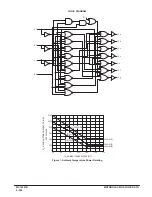
†To calculate total supply current at loads other than 50 pF:
IT(CL) = IT(50 pF) + 3.5 x 10⁻³ (CL = 50) VDDf
where: IT is in
µ
A (per package), CL in pF, VDD in V, and f in kHz is input frequency.
** The formulas given are for the typical characteristics only at 25
_
C.
This device contains circuitry to protect the inputs against damage due to high static voltages or electric fields; however, it
is advised that normal precautions be taken to avoid application of any voltage higher than maximum rated voltages to this
high impedance circuit. For proper operation it is recommended that Vin and Vout be constrained to the range VSS
v
(Vin or
Vout)
v
VDD.
Unused inputs must always be tied to an appropriate logic voltage level (e.g., either VSS or VDD).
Summary of Contents for CMOS Logic
Page 1: ......
Page 5: ...iv MOTOROLA CMOS LOGIC DATA ...
Page 6: ...Master Index 1 ...
Page 12: ...Product Selection Guide 2 ...
Page 17: ...The Better Program 3 ...
Page 20: ...B and UB Series Family Data 4 ...
Page 25: ...CMOS Handling and Design Guidelines 5 ...
Page 32: ...CMOS Handling and Design Guidelines 5 ...
Page 39: ...Data Sheets 6 ...
Page 234: ...MOTOROLA CMOS LOGIC DATA MC14174B 6 196 FUNCTIONAL BLOCK DIAGRAM TIMING DIAGRAM ...
Page 238: ...MOTOROLA CMOS LOGIC DATA MC14175B 6 200 FUNCTIONAL BLOCK DIAGRAM TIMING DIAGRAM ...
Page 555: ...CMOS Reliability 7 ...
Page 561: ...Equivalent Gate Count 8 ...
Page 563: ...Packaging Information Including Surface Mounts 9 ...
Page 571: ......