


MOTOROLA CMOS LOGIC DATA
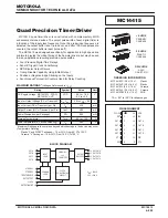
MC14490
6–212
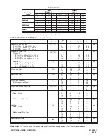
SWITCHING CHARACTERISTICS
(CL = 50 pF, TA = 25
_
C)
ÎÎÎÎÎÎÎÎÎÎÎÎÎÎÎÎ
Î
ÎÎÎÎÎÎÎÎÎÎÎÎÎÎ
Î
ÎÎÎÎÎÎÎÎÎÎÎÎÎÎÎÎ
Characteristic
ÎÎÎÎ
ÎÎÎ
Î
ÎÎÎÎ
Symbol
ÎÎÎÎÎ
Î
ÎÎÎ
Î
ÎÎÎÎÎ
VDD
Vdc
ÎÎÎÎ
Î
ÎÎ
Î
ÎÎÎÎ
Min
ÎÎÎÎ
Î
ÎÎ
Î
ÎÎÎÎ
Typ #
ÎÎÎÎ
Î
ÎÎ
Î
ÎÎÎÎ
Max
ÎÎÎ
Î
Î
Î
ÎÎÎ
Unit
ÎÎÎÎÎÎÎÎÎÎÎÎÎÎÎÎ
Î
ÎÎÎÎÎÎÎÎÎÎÎÎÎÎ
Î
ÎÎÎÎÎÎÎÎÎÎÎÎÎÎÎÎ
Output Rise Time
All Outputs
ÎÎÎÎ
ÎÎÎ
Î
ÎÎÎÎ
tTLH
ÎÎÎÎÎ
Î
ÎÎÎ
Î
ÎÎÎÎÎ
5.0
10
15
ÎÎÎÎ
Î
ÎÎ
Î
ÎÎÎÎ
—
—
—
ÎÎÎÎ
Î
ÎÎ
Î
ÎÎÎÎ
180
90
65
ÎÎÎÎ
Î
ÎÎ
Î
ÎÎÎÎ
360
180
130
ÎÎÎ
Î
Î
Î
ÎÎÎ
ns
ÎÎÎÎÎÎÎÎÎÎÎÎÎÎÎÎ
Î
ÎÎÎÎÎÎÎÎÎÎÎÎÎÎ
Î
ÎÎÎÎÎÎÎÎÎÎÎÎÎÎÎÎ
Output Fall Time
Oscillator Output
ÎÎÎÎ
ÎÎÎ
Î
ÎÎÎÎ
tTHL
ÎÎÎÎÎ
Î
ÎÎÎ
Î
ÎÎÎÎÎ
5.0
10
15
ÎÎÎÎ
Î
ÎÎ
Î
ÎÎÎÎ
—
—
—
ÎÎÎÎ
Î
ÎÎ
Î
ÎÎÎÎ
100
50
40
ÎÎÎÎ
Î
ÎÎ
Î
ÎÎÎÎ
200
100
80
ÎÎÎ
Î
Î
Î
ÎÎÎ
ns
ÎÎÎÎÎÎÎÎÎÎÎÎÎÎÎÎ
Î
ÎÎÎÎÎÎÎÎÎÎÎÎÎÎ
Î
ÎÎÎÎÎÎÎÎÎÎÎÎÎÎÎÎ
Debounce Outputs
ÎÎÎÎ
ÎÎÎ
Î
ÎÎÎÎ
tTHL
ÎÎÎÎÎ
Î
ÎÎÎ
Î
ÎÎÎÎÎ
5.0
10
15
ÎÎÎÎ
Î
ÎÎ
Î
ÎÎÎÎ
—
—
—
ÎÎÎÎ
Î
ÎÎ
Î
ÎÎÎÎ
60
30
20
ÎÎÎÎ
Î
ÎÎ
Î
ÎÎÎÎ
120
60
40
ÎÎÎ
Î
Î
Î
ÎÎÎ
ÎÎÎÎÎÎÎÎÎÎÎÎÎÎÎÎ
Î
ÎÎÎÎÎÎÎÎÎÎÎÎÎÎ
Î
Î
ÎÎÎÎÎÎÎÎÎÎÎÎÎÎ
Î
ÎÎÎÎÎÎÎÎÎÎÎÎÎÎÎÎ
Propagation Delay Time
Oscillator Input to Debounce Outputs
ÎÎÎÎ
ÎÎÎ
Î
ÎÎÎ
Î
ÎÎÎÎ
tPHL
ÎÎÎÎÎ
Î
ÎÎÎ
Î
Î
ÎÎÎ
Î
ÎÎÎÎÎ
5.0
10
15
ÎÎÎÎ
Î
ÎÎ
Î
Î
ÎÎ
Î
ÎÎÎÎ
—
—
—
ÎÎÎÎ
Î
ÎÎ
Î
Î
ÎÎ
Î
ÎÎÎÎ
285
120
95
ÎÎÎÎ
Î
ÎÎ
Î
Î
ÎÎ
Î
ÎÎÎÎ
570
240
190
ÎÎÎ
Î
Î
Î
Î
Î
Î
ÎÎÎ
ns
ÎÎÎÎÎÎÎÎÎÎÎÎÎÎÎÎ
Î
ÎÎÎÎÎÎÎÎÎÎÎÎÎÎ
Î
ÎÎÎÎÎÎÎÎÎÎÎÎÎÎÎÎ
ÎÎÎÎ
ÎÎÎ
Î
ÎÎÎÎ
tPLH
ÎÎÎÎÎ
Î
ÎÎÎ
Î
ÎÎÎÎÎ
5.0
10
15
ÎÎÎÎ
Î
ÎÎ
Î
ÎÎÎÎ
—
—
—
ÎÎÎÎ
Î
ÎÎ
Î
ÎÎÎÎ
370
160
120
ÎÎÎÎ
Î
ÎÎ
Î
ÎÎÎÎ
740
320
240
ÎÎÎ
Î
Î
Î
ÎÎÎ
ÎÎÎÎÎÎÎÎÎÎÎÎÎÎÎÎ
Î
ÎÎÎÎÎÎÎÎÎÎÎÎÎÎ
Î
ÎÎÎÎÎÎÎÎÎÎÎÎÎÎÎÎ
Clock Frequency (50% Duly Cycle)
(External Clock)
ÎÎÎÎ
ÎÎÎ
Î
ÎÎÎÎ
fcl
ÎÎÎÎÎ
Î
ÎÎÎ
Î
ÎÎÎÎÎ
5.0
10
15
ÎÎÎÎ
Î
ÎÎ
Î
ÎÎÎÎ
—
—
—
ÎÎÎÎ
Î
ÎÎ
Î
ÎÎÎÎ
2.8
6
9
ÎÎÎÎ
Î
ÎÎ
Î
ÎÎÎÎ
1.4
3.0
4.5
ÎÎÎ
Î
Î
Î
ÎÎÎ
MHz
ÎÎÎÎÎÎÎÎÎÎÎÎÎÎÎÎ
Î
ÎÎÎÎÎÎÎÎÎÎÎÎÎÎ
Î
ÎÎÎÎÎÎÎÎÎÎÎÎÎÎÎÎ
Setup Time (See Figure 1)
ÎÎÎÎ
ÎÎÎ
Î
ÎÎÎÎ
tsu
ÎÎÎÎÎ
Î
ÎÎÎ
Î
ÎÎÎÎÎ
5.0
10
15
ÎÎÎÎ
Î
ÎÎ
Î
ÎÎÎÎ
100
80
60
ÎÎÎÎ
Î
ÎÎ
Î
ÎÎÎÎ
50
40
30
ÎÎÎÎ
Î
ÎÎ
Î
ÎÎÎÎ
—
—
—
ÎÎÎ
Î
Î
Î
ÎÎÎ
ns
ÎÎÎÎÎÎÎÎÎÎÎÎÎÎÎÎ
Î
ÎÎÎÎÎÎÎÎÎÎÎÎÎÎ
Î
ÎÎÎÎÎÎÎÎÎÎÎÎÎÎÎÎ
Maximum External Clock Input
Rise and Fall Time
Oscillator Input
ÎÎÎÎ
ÎÎÎ
Î
ÎÎÎÎ
tr, tf
ÎÎÎÎÎ
Î
ÎÎÎ
Î
ÎÎÎÎÎ
5.0
10
15
ÎÎÎÎÎÎÎÎÎÎ
Î
ÎÎÎÎÎÎÎÎ
Î
ÎÎÎÎÎÎÎÎÎÎ
No Limit
ÎÎÎ
Î
Î
Î
ÎÎÎ
ns
ÎÎÎÎÎÎÎÎÎÎÎÎÎÎÎÎ
Î
ÎÎÎÎÎÎÎÎÎÎÎÎÎÎ
Î
Î
ÎÎÎÎÎÎÎÎÎÎÎÎÎÎ
Î
Î
ÎÎÎÎÎÎÎÎÎÎÎÎÎÎ
Î
Î
ÎÎÎÎÎÎÎÎÎÎÎÎÎÎ
Î
ÎÎÎÎÎÎÎÎÎÎÎÎÎÎÎÎ
Oscillator Frequency
OSCout
Cext
≥
100 pF*
Note: These equations are intended to be a design guide.
Laboratory experimentation may be required. Formulas
are typically
±
15% of actual frequencies.
ÎÎÎÎ
ÎÎÎ
Î
ÎÎÎ
Î
ÎÎÎ
Î
ÎÎÎ
Î
ÎÎÎÎ
fosc, typ
ÎÎÎÎÎ
Î
ÎÎÎ
Î
Î
ÎÎÎ
Î
Î
ÎÎÎ
Î
Î
ÎÎÎ
Î
ÎÎÎÎÎ
5.0
10
15
ÎÎÎÎÎÎÎÎÎÎ
Î
ÎÎÎÎÎÎÎÎ
Î
Î
ÎÎÎÎÎÎÎÎ
Î
Î
ÎÎÎÎÎÎÎÎ
Î
Î
ÎÎÎÎÎÎÎÎ
Î
ÎÎÎÎÎÎÎÎÎÎ
ÎÎÎ
Î
Î
Î
Î
Î
Î
Î
Î
Î
Î
Î
Î
ÎÎÎ
Hz
* The formulas given are for the typical characteristics only at 25
_
C.
#Data labelled “Typ” is not to be used for design purposes but is intended as an indication of the IC’s potential performance.
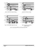
*POWER–DOWN CONSIDERATIONS
Large values of Cext may cause problems when powering down the MC14490 because of the amount of energy stored in the
capacitor. When a system containing this device is powered down, the capacitor may discharge through the input protection
diodes at Pin 7 or the parasitic diodes at Pin 9. Current through these internal diodes must be limited to 10 mA, therefore the
turn–off time of the power supply must not be faster than t = (VDD – VSS)
Cext/(10 mA). For example, If VDD – VSS = 15 V and
Cext = 1
µ
F, the power supply must turn off no faster than t = (15 V)
(1
µ
F) / 10 mA = 1.5 ms. This is usually not a problem
because power supplies are heavily filtered and cannot discharge at this rate.
When a more rapid decrease of the power supply to zero volts occurs, the MC14490 may sustain damage. To avoid this possi-
bility, use external clamping diodes, D1 and D2, connected as shown in Figure 2.
Figure 1. Switching Waveforms
Figure 2. Discharge Protection During Power Down
OSCin
Aout
Aout
OSCin
Ain
VDD
0 V
VDD
0 V
VDD
0 V
50%
90%
50%
10%
tr
tf
tPHL
90%
10%
50%
50%
tsu
50%
D1
D2
Cext
9
7
OSCin
OSCout
MC14490
tPLH
VDD
VDD
1.5
Cext (in
µ
F)
4.5
Cext (in
µ
F)
6.5
Cext (in
µ
F)
Summary of Contents for CMOS Logic
Page 1: ......
Page 5: ...iv MOTOROLA CMOS LOGIC DATA ...
Page 6: ...Master Index 1 ...
Page 12: ...Product Selection Guide 2 ...
Page 17: ...The Better Program 3 ...
Page 20: ...B and UB Series Family Data 4 ...
Page 25: ...CMOS Handling and Design Guidelines 5 ...
Page 32: ...CMOS Handling and Design Guidelines 5 ...
Page 39: ...Data Sheets 6 ...
Page 234: ...MOTOROLA CMOS LOGIC DATA MC14174B 6 196 FUNCTIONAL BLOCK DIAGRAM TIMING DIAGRAM ...
Page 238: ...MOTOROLA CMOS LOGIC DATA MC14175B 6 200 FUNCTIONAL BLOCK DIAGRAM TIMING DIAGRAM ...
Page 555: ...CMOS Reliability 7 ...
Page 561: ...Equivalent Gate Count 8 ...
Page 563: ...Packaging Information Including Surface Mounts 9 ...
Page 571: ......