


MOTOROLA CMOS LOGIC DATA
6–41
MC14015B
Dual 4-Bit Static Shift Register
The MC14015B dual 4–bit static shift register is constructed with MOS
P–channel and N–channel enhancement mode devices in a single
monolithic structure. It consists of two identical, independent 4–state
serial–input/parallel–output registers. Each register has independent Clock
and Reset inputs with a single serial Data input. The register states are type
D master–slave flip–flops. Data is shifted from one stage to the next during
the positive–going clock transition. Each register can be cleared when a high
level is applied on the Reset line. These complementary MOS shift registers
find primary use in buffer storage and serial–to–parallel conversion where
low power dissipation and/or noise immunity is desired.
•
Diode Protection on All Inputs
•
Supply Voltage Range = 3.0 Vdc to 18 Vdc
•
Logic Edge–Clocked Flip–Flop Design —
Logic state is retained indefinitely with clock level either high or low;
information is transferred to the output only on the positive going edge
of the clock pulse.
•
Capable of Driving Two Low–power TTL Loads or One Low–power
Schottky TTL Load Over the Rated Temperature Range.
ÎÎÎÎÎÎÎÎÎÎÎÎÎÎÎÎÎÎÎÎÎ
ÎÎÎÎÎÎÎÎÎÎÎÎÎÎÎÎÎÎÎÎÎ
MAXIMUM RATINGS*
(Voltages Referenced to VSS)
ÎÎÎÎ
ÎÎÎÎ
Symbol
ÎÎÎÎÎÎÎÎÎÎÎ
ÎÎÎÎÎÎÎÎÎÎÎ
Parameter
ÎÎÎÎÎÎ
ÎÎÎÎÎÎ
Value
ÎÎÎ
ÎÎÎ
Unit
ÎÎÎÎ
ÎÎÎÎ
VDD
ÎÎÎÎÎÎÎÎÎÎÎ
ÎÎÎÎÎÎÎÎÎÎÎ
DC Supply Voltage
ÎÎÎÎÎÎ
ÎÎÎÎÎÎ
– 0.5 to + 18.0
ÎÎÎ
ÎÎÎ
V
ÎÎÎÎ
ÎÎÎÎ
Vin, Vout
ÎÎÎÎÎÎÎÎÎÎÎ
ÎÎÎÎÎÎÎÎÎÎÎ
Input or Output Voltage (DC or Transient)
ÎÎÎÎÎÎ
ÎÎÎÎÎÎ
– 0.5 to VDD + 0.5
ÎÎÎ
ÎÎÎ
V
ÎÎÎÎ
ÎÎÎÎ
lin, lout
ÎÎÎÎÎÎÎÎÎÎÎ
ÎÎÎÎÎÎÎÎÎÎÎ
Input or Output Current (DC or Transient),
per Pin
ÎÎÎÎÎÎ
ÎÎÎÎÎÎ
±
10
ÎÎÎ
ÎÎÎ
mA
ÎÎÎÎ
ÎÎÎÎ
PD
ÎÎÎÎÎÎÎÎÎÎÎ
ÎÎÎÎÎÎÎÎÎÎÎ
Power Dissipation, per Package†
ÎÎÎÎÎÎ
ÎÎÎÎÎÎ
500
ÎÎÎ
ÎÎÎ
mW
ÎÎÎÎ
ÎÎÎÎ
Tstg
ÎÎÎÎÎÎÎÎÎÎÎ
ÎÎÎÎÎÎÎÎÎÎÎ
Storage Temperature
ÎÎÎÎÎÎ
ÎÎÎÎÎÎ
– 65 to + 150
ÎÎÎ
ÎÎÎ
_
C
ÎÎÎÎ
ÎÎÎÎ
TL
ÎÎÎÎÎÎÎÎÎÎÎ
ÎÎÎÎÎÎÎÎÎÎÎ
Lead Temperature (8–Second Soldering)
ÎÎÎÎÎÎ
ÎÎÎÎÎÎ
260
ÎÎÎ
ÎÎÎ
_
C
* Maximum Ratings are those values beyond which damage to the device may occur.
†Temperature Derating:
Plastic “P and D/DW” Packages: – 7.0 mW/
_
C From 65
_
C To 125
_
C
Ceramic “L” Packages: – 12 mW/
_
C From 100
_
C To 125
_
C
TRUTH TABLE
C
D
R
Q0
Qn
0
0
0
Qn–1
1
0
1
Qn–1
X
0
No Change
No Change
X
X
1
0
0
X = Don’t Care
Qn = Q0, Q1, Q2, or Q3, as applicable.
Qn–1 = Output of prior stage.
MOTOROLA
SEMICONDUCTOR TECHNICAL DATA
MC14015B
L SUFFIX
CERAMIC
CASE 620
ORDERING INFORMATION
MC14XXXBCP
Plastic
MC14XXXBCL
Ceramic
MC14XXXBD
SOIC
TA = – 55
°
to 125
°
C for all packages.
P SUFFIX
PLASTIC
CASE 648
D SUFFIX
SOIC
CASE 751B
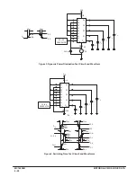
BLOCK DIAGRAM
14
1
15
6
9
7
5
4
3
10
13
12
11
2
Q0
Q1
Q2
Q3
Q0
Q1
Q2
Q3
D
C
R
R
D
C
VDD = PIN 16
VSS = PIN 8
Summary of Contents for CMOS Logic
Page 1: ......
Page 5: ...iv MOTOROLA CMOS LOGIC DATA ...
Page 6: ...Master Index 1 ...
Page 12: ...Product Selection Guide 2 ...
Page 17: ...The Better Program 3 ...
Page 20: ...B and UB Series Family Data 4 ...
Page 25: ...CMOS Handling and Design Guidelines 5 ...
Page 32: ...CMOS Handling and Design Guidelines 5 ...
Page 39: ...Data Sheets 6 ...
Page 234: ...MOTOROLA CMOS LOGIC DATA MC14174B 6 196 FUNCTIONAL BLOCK DIAGRAM TIMING DIAGRAM ...
Page 238: ...MOTOROLA CMOS LOGIC DATA MC14175B 6 200 FUNCTIONAL BLOCK DIAGRAM TIMING DIAGRAM ...
Page 555: ...CMOS Reliability 7 ...
Page 561: ...Equivalent Gate Count 8 ...
Page 563: ...Packaging Information Including Surface Mounts 9 ...
Page 571: ......